Get "10 RF Design Principles Every Engineer Should Know" Free
Learn practical principles for better RF circuits, PCB layouts, simulations, measurements, and troubleshooting.

Learn how to read antenna radiation patterns, including main lobes, side lobes, nulls, beamwidth, polar plots, and PCB integration effects.
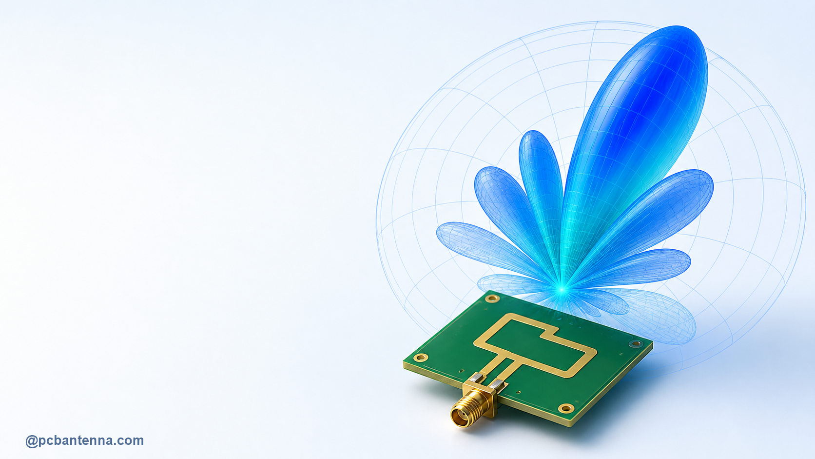
An antenna radiation pattern, sometimes called a radiation diagram, shows where an antenna sends or receives energy most effectively. It is one of the most useful pictures in RF engineering because it turns a vague question, such as “Will this antenna cover the whole room?”, into something that can be checked: which directions are strong, which directions are weak, and how wide the useful beam really is.
This guide explains the parts of an antenna radiation pattern, how to read lobes, nulls, beamwidth, and polar plots, and how to use the result in a real PCB antenna design. The goal is not to memorize a pretty plot. It is to choose coverage that works once the antenna is inside the product.
A radiation pattern describes the angular distribution of radiated field, power, or gain around an antenna. It is normally taken in the far field, far enough away that the shape of the field no longer depends strongly on the measurement distance. The pattern is always tied to a frequency, a polarization, and a defined antenna or product configuration. Change any of those, and the pattern can change too.
Patterns are commonly shown as a full 3D shape or as one or more 2D cuts through that shape. A 3D view gives an excellent overall impression. A 2D cut is often easier to compare because it clearly shows angles and relative levels. A good datasheet or simulation report should say which plane is shown and whether values are normalized to the pattern peak or shown as absolute gain.
The main lobe is the direction of strongest radiation. A directional antenna deliberately puts most of its useful energy in this lobe. In a point-to-point link, this can improve the desired signal. In a device that moves around, a narrow main lobe can become a problem when the device turns away from the access point.
Side lobes are smaller peaks away from the main lobe. They are not automatically bad; every practical pattern has trade-offs. But strong side lobes can direct energy into areas where it is not needed, pick up interference, or make a coverage area less predictable. A back lobe is radiation behind the intended forward direction. It matters for wall-mounted, panel, and array antennas where rear coverage or interference must be controlled.
A null is a direction where radiation falls to a very low level. Nulls are often more important than the peak of the pattern because a receiver that sits in one can lose a link even when the advertised gain looks impressive. Small changes to a product ground plane, a battery, cable routing, or enclosure can shift a null enough to matter in use.
Half-power beamwidth, often written HPBW, is the angular width between the two points where the main lobe has dropped by 3 dB from its peak. A 3 dB reduction corresponds to half the radiated power density, which makes HPBW a practical way to describe the usable width of a directional pattern. A smaller HPBW usually means a more focused beam; a larger HPBW gives broader coverage.
You may also see first-null beamwidth, measured between the first nulls either side of a main lobe. It can be helpful for comparing patterns, but it is not a replacement for HPBW and may be less clear when a pattern does not have clean, deep nulls. For coverage planning, study both the stated beamwidth and the full polar plot rather than relying on one number.
A polar plot uses angle around the center and level as distance from the center. It makes directional shape immediately visible: a broad circle suggests wide coverage, while a strong teardrop suggests a forward-directed antenna. A Cartesian plot places angle on the horizontal axis and gain or field level on the vertical axis. It is usually easier to read exact beamwidth, side-lobe level, and null depth from this form.
Before comparing two plots, check the scale. A normalized plot sets the peak to 0 dB and shows relative changes; it does not tell you the actual peak gain. An absolute plot may show dBi or another stated quantity. Linear and decibel scales can also make the same data look very different. The labels, frequency, and reference must match before the comparison means anything.
For linearly polarized antennas, reports often include two principal cuts called the E-plane and H-plane. The E-plane contains the electric-field polarization direction; the H-plane is the orthogonal principal plane. These names are useful shorthand, but the coordinate system still needs to be stated. On a PCB antenna, the board orientation, connector direction, and ground-plane shape all affect what the pattern means in the final product.
Do not assume an antenna described as “omnidirectional” is equally strong in every 3D direction. A vertical dipole-like pattern, for example, can be broad around the horizon while having nulls above and below the antenna. That can be perfect for a device on the same floor and poor for a link directly overhead.
It is tempting to use a low S11 value as proof that an antenna is working well. S11 and return loss are valuable measurements of input match, but they do not reveal where the antenna radiates, how efficiently it radiates, or whether the strongest lobe points in the required direction. Our guide to S11 and return loss explains what the measurement does tell you.
For a useful antenna assessment, review impedance match, efficiency, realized gain, polarization, and the radiation pattern together. The antenna gain guide explains why peak gain without directional context can be misleading, while antenna polarization covers another common source of link loss.
A clean evaluation board is only the beginning. A PCB antenna’s radiation pattern can be altered by the board ground plane, metal shielding, battery, display, housing, USB cable, mounting surface, and the user’s hand or body. A pattern that looks balanced in free space may be tilted, blocked, or split into unexpected lobes after integration. This is why final validation should happen with the intended enclosure and nearby components in place.
Start with sound layout practice from PCB Antenna Design Basics, then use full-wave simulation to investigate sensitive changes before hardware is built. Our HFSS antenna simulation workflow shows a practical route from geometry to far-field results. Simulation helps you understand a model; measurement confirms the finished product.
For early calculations, the RF Link Budget Calculator and Free Space Path Loss Calculator can help turn an intended coverage direction into a realistic power estimate. The full PCB Antenna calculator collection is useful for the dimensions and RF quantities that feed the wider design process.
A radiation pattern is the map that tells you where antenna performance will be available and where it will not. Main lobes, side lobes, nulls, beamwidth, and polarization are all parts of that map. When they are reviewed alongside matching, efficiency, and a realistic link budget, you get a much stronger basis for an antenna decision than a single gain number can provide. For design review, simulation, or final-product validation, explore our antenna design services or contact PCB Antenna.