Get "10 RF Design Principles Every Engineer Should Know" Free
Learn practical principles for better RF circuits, PCB layouts, simulations, measurements, and troubleshooting.

A practical HFSS antenna simulation workflow covering geometry, materials, ports, boundaries, meshing, sweeps, and measurement validation.
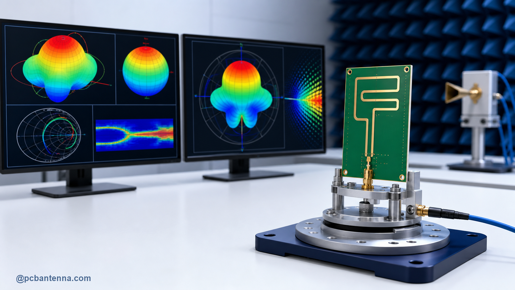
HFSS antenna simulation is most useful when it answers a specific design question. Will this PCB antenna resonate in the target band? Does the enclosure shift the match? Is the ground plane helping or hurting? Which trace length gives the best trade-off between bandwidth and efficiency? When the model is built around those questions, simulation can save several prototype rounds. When it is built as a beautiful 3D picture with missing product details, it can create a very confident wrong answer.
This guide gives a practical HFSS antenna simulation workflow, from first geometry to results you can compare with hardware. The same habits apply to many full-wave electromagnetic tools, but the examples are written with PCB antennas and HFSS-style setup decisions in mind.
Before opening HFSS, decide what you are trying to learn. A first-pass PCB antenna model does not need every screw, label, and connector. It does need the features that control the RF behavior you are studying: board outline, layer stackup, main ground plane, antenna trace, feed, nearby metal, and the enclosure or battery if they are close enough to matter.
Write down a small set of outputs before modeling. For example:
That list keeps the project focused. It also tells you what must be present in the model. If the goal is to compare two antenna locations inside a plastic enclosure, leaving out the enclosure defeats the purpose. If the goal is only to tune a bare PCB trace, begin with the board and feed, then add complexity after the basic model behaves sensibly.
A parametric model is easier to trust and far easier to tune. Instead of drawing a fixed trace, create named variables for dimensions you expect to explore: antenna length, meander spacing, feed offset, shorting position, ground clearance, substrate thickness, or enclosure gap. Use clear names and units. Six weeks later, antenna_length is much more useful than a sketch dimension with no context.
For a PCB antenna, include the board outline and copper layers that influence the current path. A perfectly isolated radiator usually tells you less than a simplified but realistic board. The ground plane is especially important. In compact designs, it often participates strongly in resonance and radiation, so trimming it, splitting it, or adding a large connector can change the answer even when the antenna trace is untouched.
Use the Wavelength Calculator and Antenna Length Calculator for a rough physical scale before you start. These tools will not produce the finished HFSS dimensions, but they help you spot an impossible starting geometry and choose a sensible sweep range.
Material assignments are easy to rush and expensive to ignore. The dielectric properties and thickness of the PCB affect the electrical size of traces and the behavior of the feed. Copper thickness, solder mask, adhesive layers, plastic enclosures, foam, batteries, and nearby metal may matter too, depending on the design.
Use the fabricator’s stackup and material data when they are available. If you only have an early generic stackup, label it as an assumption and plan to update the model once the board is specified. Do not treat every FR-4 board as electrically identical, especially when the antenna is small, narrowband, or operating at higher frequencies. A model can be geometrically perfect and still miss the target if its materials are only guesses.
The port definition is where the simulated structure becomes a driven antenna. A bad port can produce an S11 curve that looks smooth but does not represent the physical feed. Choose a port type that matches the geometry you are modeling. A wave port is often appropriate where a transmission line enters a model with a clear cross-section. A lumped port can be useful for a localized feed gap or compact excitation, provided its reference direction and integration line are set deliberately.
Check the return path as carefully as the signal conductor. On a PCB feed, the ground reference is part of the port definition and part of the real RF circuit. If the model has no credible current return, the simulated input impedance may not map to the board you will measure. This is also why a coax connector, launch, or short feed section sometimes deserves inclusion in a higher-fidelity model.
After the first solve, inspect input impedance as well as S11. If the impedance behavior is surprising, look at surface current around the port and feed before adding matching components. Matching can improve the numerical S11 result while leaving an incorrect or badly modeled current path hidden underneath.
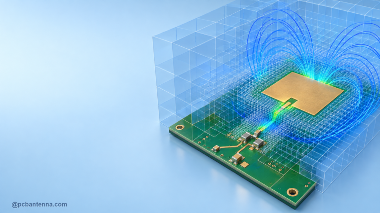
An antenna radiates into open space, so the simulation needs an appropriate outer region and radiation treatment. In HFSS, that commonly means an air volume around the product together with a radiation or open boundary approach suitable for the analysis. The needed spacing and boundary choice depend on frequency, geometry, and solver setup. There is no one distance that is safe for every design.
Keep the outer region large enough that the near fields around the antenna are not being artificially constrained. If moving the boundary materially changes the result, the model is giving you useful feedback: the boundary setup was still influencing the antenna. For symmetric structures, symmetry planes can reduce solve time, but only use them when the excitation and fields genuinely satisfy the assumed symmetry.
Pick an adaptive solution frequency that supports the physics you care about, then define a sweep that covers the full operating band with margin. The exact setup depends on whether you are working on a narrowband antenna, a multiband structure, or a wideband/UWB design. The important part is not a fixed recipe. It is ensuring that the mesh refinement and sweep resolution are sufficient to capture the resonances and impedance movement you intend to trust.
Watch convergence rather than assuming a successful solve is a validated solve. Compare successive adaptive passes, review the change in key outputs, and inspect the mesh in small RF-critical regions such as narrow gaps, feed transitions, vias, and shorting connections. An overly coarse representation can miss a local capacitance or inductance that shifts the final tune. An unnecessarily fine mesh everywhere can make the project slow without improving the decision.
Start with the simplest outputs. Review S11 or return loss across frequency, then the input impedance. Next, inspect surface current at the frequencies you care about. Current plots often reveal whether the intended radiator and ground are doing the work, or whether a connector, cable model, or unintended metal region has become the dominant path.
Once the current distribution makes sense, move to far-field outputs. Check realized gain, radiation pattern, polarization, and efficiency in the directions that matter for the product. A low S11 value is useful, but it is not a guarantee of good radiation. Accepted power can still disappear into dielectric loss, conductor loss, or unwanted coupling. Our S11 and return loss guide explains this distinction in more detail.
Use plots as a debugging tool, not just a report graphic. If the pattern changes unexpectedly when you add the enclosure, inspect current on the enclosure and ground. If efficiency drops after adding a battery, look at field concentration and coupling near the battery boundary. Those observations are often more actionable than the final dB number alone.
Parametric sweeps are powerful because they turn a static model into a design map. Sweep one or two high-impact variables first: trace length, feed position, short position, ground clearance, or a matching component value. Record how the resonant frequency, bandwidth, impedance, and efficiency change. A small sweep that explains the structure is more valuable than a huge blind optimization with no engineering story behind it.
When the design is close, use narrower ranges and finer steps. When it is far from target, change the geometry in a meaningful way before spending time on optimization. Keep a short decision log: what changed, why it changed, which output moved, and what you will test next. That makes it much easier to reconcile HFSS results with the eventual prototype.
A simulation becomes genuinely valuable when it predicts a measurement closely enough to guide the next design decision. Build the first prototype with tuning access, measure the same quantities you simulated, and compare assumptions before changing the model. Match the reference plane between simulation and VNA measurement as closely as practical. Include the real enclosure, battery, cable arrangement, and major metal features in both test and model when they are relevant.
Expect differences. Board material variation, connector launches, solder, mechanical tolerances, and unmodeled details can all move a result. The goal is not to force the measurement to look like HFSS. The goal is to discover which assumption needs improving so the next simulation becomes more predictive. For a worked design-and-measure flow, read UWB PCB Antenna Design and Simulation in HFSS.
When the antenna model is close, connect the results to the actual wireless requirement. Gain, efficiency, polarization loss, cable loss, and free-space path loss all affect whether the link has margin. The RF Link Budget Calculator, Free Space Path Loss Calculator, and Antenna Gain Calculator can help turn a simulation output into a useful product-level check.
HFSS is at its best when it helps you make the next physical choice with less guesswork. Model the right things, verify the feed and boundary assumptions, inspect current before celebrating a chart, and keep the final product in the loop. If you need help setting up a model, comparing it with measurements, or getting an antenna project ready for validation, see our engineering services or contact PCB Antenna.