Get "10 RF Design Principles Every Engineer Should Know" Free
Learn practical principles for better RF circuits, PCB layouts, simulations, measurements, and troubleshooting.

Compare CST and HFSS for practical antenna simulation workflows, including geometry, convergence, optimization, post-processing, and validation.
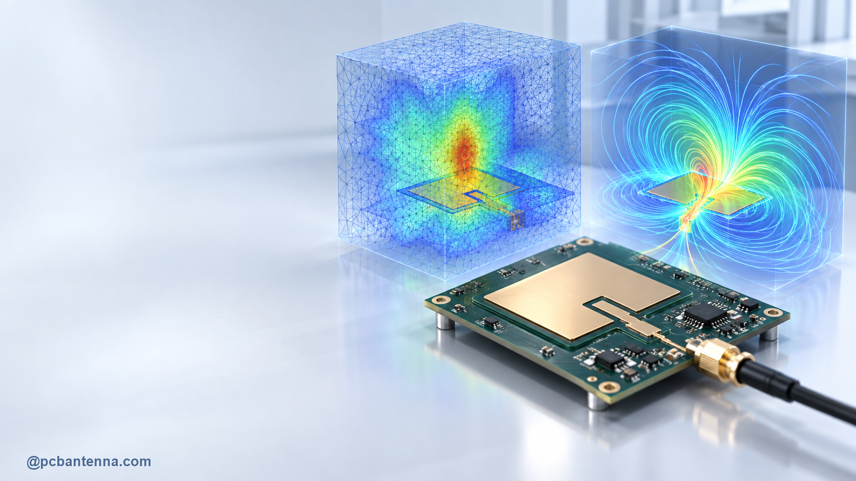
CST and HFSS are both widely used electromagnetic simulation environments for antenna work. The better choice is rarely decided by a product brochure. It depends on the antenna type, frequency range, available solver expertise, model size, required outputs, licensing, workflow around CAD data, and how the results will be validated in the lab.
The useful comparison is not “Which solver is best?” It is “Which workflow helps this team make a reliable decision with the available time and data?” A careful model in either environment is more valuable than an advanced tool used with unrealistic materials, poor ports, or an incomplete enclosure.
Define the design question first. Are you tuning a narrowband PCB antenna, exploring a broad frequency range, studying a handset with complex mechanics, comparing an array, or checking coupling between several antennas? The geometry and outputs should drive the solver setup, mesh strategy, and validation plan.
For simple PCB antennas, the greatest source of error is often not the solver brand. It is an incorrect stackup, missing solder mask, simplified ground plane, unrealistic connector, or omitted battery and enclosure. Get the basic model right before comparing run times.
HFSS is often used for full-wave electromagnetic analysis of antenna structures, feeds, packages, and related RF components. Its adaptive meshing workflow gives engineers a direct way to check whether a solution is converging. Ansys documents single-frequency, multi-frequency, and broadband adaptive strategies, which can be selected to suit the frequency problem being studied.
For a PCB antenna, this makes the review discipline clear: inspect the final adaptive passes, test whether the selected frequency strategy covers the required band, and avoid declaring victory from one attractive S11 curve. Our HFSS mesh convergence guide explains that process in detail.
CST is also commonly chosen for antenna design and can be a strong fit when its modeling, solver options, integration with a team’s existing design flow, and post-processing tools match the problem. The important work is the same: make the geometry honest, choose an appropriate frequency and boundary setup, check numerical stability, and compare the result with measurements.
Do not switch tools merely because a preliminary model gives an inconvenient answer. First check the model, excitation, mesh, boundary, and mechanical assumptions. If a second solver is available, use it as an independent comparison for an important design, especially when the device has a complex enclosure or multiple interacting antennas.
Use the same PCB outline, material data, conductor thickness, antenna geometry, feed reference plane, enclosure model, and frequency range. Compare S11, current distribution, and a defined set of far-field cuts. Record the mesh or discretization settings and the actual compute resources used. Otherwise, a difference in results may be caused by different models rather than different solvers.
Then compare both against hardware. A calibrated VNA test for the antenna match and a suitable radiated test give the most useful reality check. If both tools disagree with the prototype in the same direction, the missing part may be the model or the measurement fixture rather than either solver.
The best tool is the one that lets the team build a repeatable chain from layout to simulation to measurement. Establish templates for materials, ports, boundaries, reports, and design reviews. Keep those templates flexible enough for the exact antenna reference layout. For a focused sweep workflow, see parametric sweep optimization for PCB antenna bandwidth.
For help selecting a simulation and validation workflow for a specific product, contact PCB Antenna.