Get "10 RF Design Principles Every Engineer Should Know" Free
Learn practical principles for better RF circuits, PCB layouts, simulations, measurements, and troubleshooting.

Learn the difference between near-field and far-field antenna testing, where VNA measurements fit, and how to choose the right RF test method.
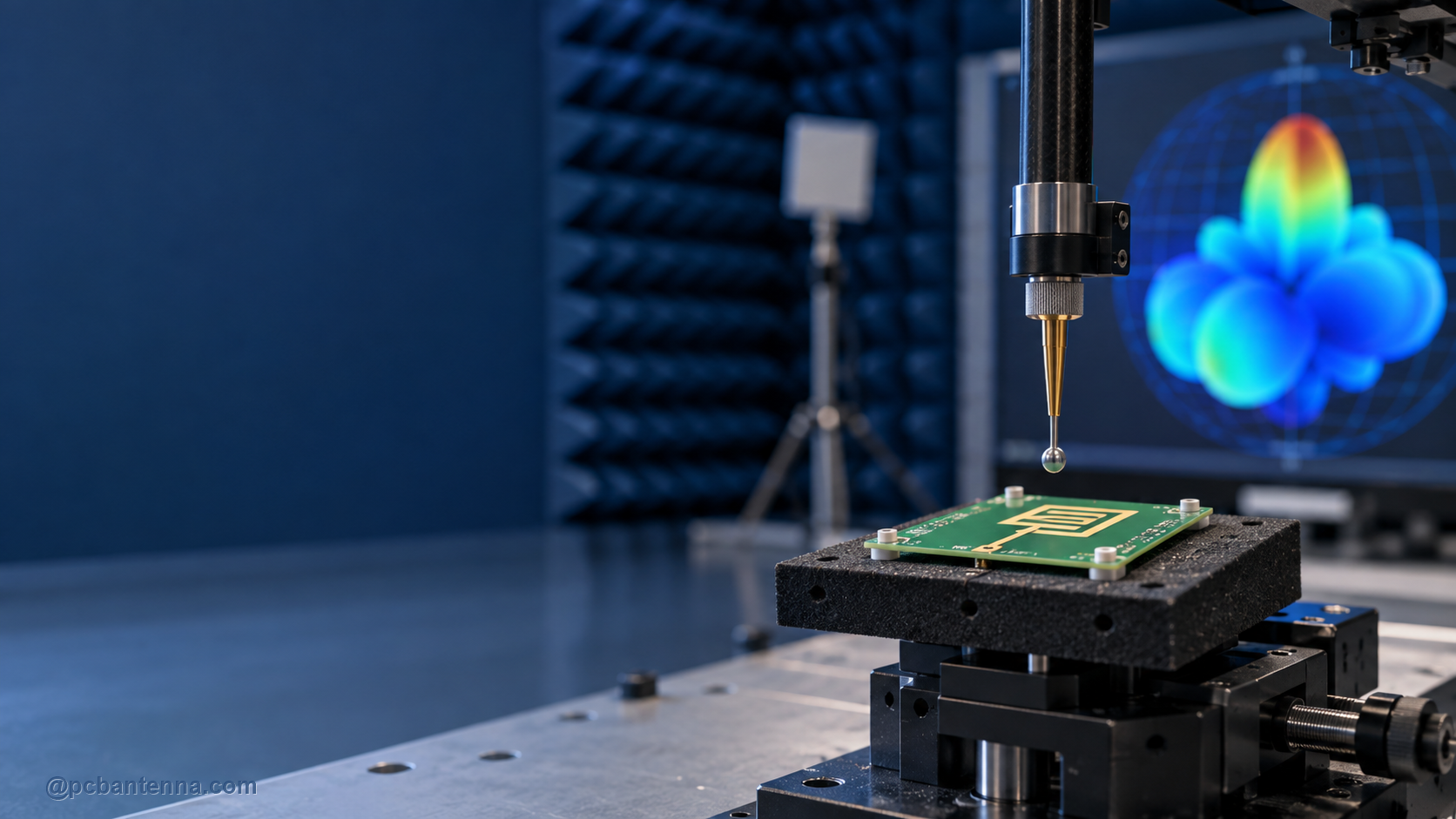
Near field and far field describe different regions around an antenna. The distinction matters because the behavior you see, the instruments you use, and the questions you can answer are different in each region. A near-field probe can be excellent for finding unwanted coupling on a PCB. It cannot, by itself, replace a far-field radiation-pattern measurement.
The near field is the region close enough to the antenna that electric and magnetic fields have not settled into the simple plane-wave relationship used for distant radiation analysis. It includes reactive energy stored around the antenna and can be strongly affected by geometry, ground plane, enclosure, cables, and nearby metal.
For PCB work, near-field investigation is useful for locating noise sources, observing coupling around a feed or matching network, comparing two layout revisions, and finding a cable or shield that interacts with the antenna. It is a diagnostic tool. It helps answer, “What is happening close to this structure?”
The far field is the region far enough from the antenna that the radiated field behaves approximately as a traveling wave and angular pattern measurements become meaningful. In this region, engineers compare gain, polarization, directivity, nulls, and coverage in a way that relates to link performance.
Far-field distance is not a single number for every antenna. It depends on wavelength and the largest dimension of the radiating structure. Test facilities calculate an appropriate separation based on the antenna under test and the desired measurement accuracy. For small antennas, the physical test range may still need enough room to reduce reflections and unwanted coupling.
A one-port VNA measurement of S11 is neither a near-field scan nor a far-field pattern test. It measures the reflection seen at the antenna feed. It is invaluable for checking match, tuning, and repeatability, but it does not directly reveal the full radiation pattern or total efficiency.
Use S11 along with the appropriate field measurement. A stable S11 curve can coexist with a poor pattern if nearby mechanical parts absorb, block, or redirect radiation. Conversely, a pattern improvement may require a matching adjustment to restore the intended band. See VSWR, return loss, and S11 explained for the port-measurement side.
Do not leave a test cable hanging beside the antenna and assume it has no effect. Keep cable routing repeatable, use the correct calibration reference plane, and avoid letting a metal fixture enter the antenna’s main field region. For small antennas, a hand, battery, or enclosure can matter as much as the board itself.
When comparing designs, change one item at a time. First compare bare boards, then add the enclosure, then the battery, then the normal use condition. This isolates the source of a pattern or match change. The workflow is slower than a single quick test, but much faster than guessing through several board revisions.
Simulation can show near fields, surface currents, and far-field patterns in the same project, but only if the geometry and boundaries are realistic. Review a simulation with the same frequency range, orientation, and enclosure assumptions that will be used in the lab. Our guide to HFSS far-field radiation patterns is a useful starting point.
Use the measurement that answers the actual product question. If the device has a range problem in one orientation, a far-field comparison may be decisive. If a switching regulator is coupling into the RF feed, a near-field scan can find it quickly. For professional testing support, contact PCB Antenna.