Get "10 RF Design Principles Every Engineer Should Know" Free
Learn practical principles for better RF circuits, PCB layouts, simulations, measurements, and troubleshooting.

Design a reliable 2.4 GHz printed monopole antenna with practical guidance on ground plane, keepout, 50-ohm feed, matching, tuning, and validation.

A printed monopole is one of the most useful antenna options for a 2.4 GHz PCB: it is low cost, easy to manufacture with the board, and easy to adjust during a prototype cycle. It is also easy to get wrong. A trace that resembles a quarter-wave antenna on a screenshot can still perform poorly when its ground plane, feed line, enclosure, battery, or keepout area changes.
This guide covers a practical printed monopole antenna design process for 2.4 GHz Bluetooth, Wi-Fi, Thread, Zigbee, and similar devices. It explains the starting geometry, ground-plane relationship, layout details, tuning workflow, and validation steps that turn a trace into an antenna system you can trust.
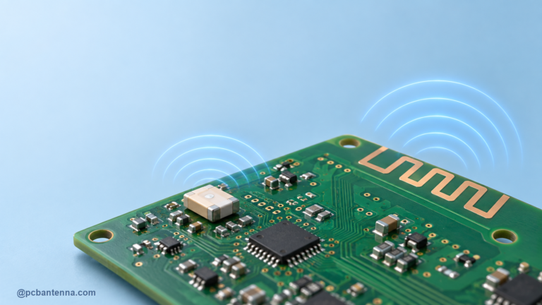
A monopole is an antenna element fed against a ground reference. In a common 2.4 GHz PCB implementation, the visible trace is approximately a quarter wavelength electrically and the board ground plane acts as the other part of the radiating system. TI describes this relationship as a quarter-wave monopole using the ground plane as an effective second quarter-wave element.
At 2.4 GHz, the free-space wavelength is about 125 mm, so a free-space quarter wavelength is around 31 mm. That value is a useful first check, not a finished layout length. A printed trace experiences dielectric loading, bends, the nearby ground edge, the feed transition, and surrounding objects. Most real PCB monopoles therefore begin from a proven reference layout or a simulated first pass, then are tuned on representative hardware.
Start by defining what the antenna must cover. A 2.4 GHz product may need the full Wi-Fi band, Bluetooth channels, or multiple protocols with different link and orientation expectations. Note the intended board size, enclosure, battery position, cables, and metal parts. A small sensor hanging freely, a wall-mounted device, and a handheld product can all require different pattern priorities even when they use the same radio chip.
Choose a feed location at a board edge where the antenna can have a clear keepout region. A quarter-wave monopole works with its ground system, so moving it to the middle of a crowded board is rarely a neutral layout change. Keep the antenna area away from noisy digital routing, switching inductors, displays, shields, and battery metal as much as the product allows.
The ground plane is not just a return path in a monopole design. It is part of the radiating structure and strongly affects input impedance, efficiency, resonance, and pattern. Nordic’s 2.45 GHz printed-monopole guidance explicitly calls the antenna ground-plane dependent and notes that it needs a single-ended feed.
Use a coherent, well-connected ground region on the board side opposite the monopole. Connect relevant ground layers with stitching vias and make the return path around the RF feed intentional. Then stop the ground plane at the antenna keepout boundary. Avoid copper pours, planes, random traces, or vias directly below and around the radiating trace unless the reference design specifically includes them.
Do not apply a one-size-fits-all “bigger ground is always better” rule. Board proportions and the antenna position determine how the ground participates. Copying a validated reference layout means copying the antenna trace, ground edge, keepout, feed, stackup assumptions, and matching network together. The PCB antenna ground-plane guide explains why partial copying usually fails.
Route the RF output to the monopole with a controlled-impedance feed appropriate for the board stackup, such as microstrip or grounded coplanar waveguide. Keep the RF trace short, direct, and consistently referenced to ground. Do not route unrelated digital signals beside it or create abrupt geometry changes immediately before the antenna.
Leave a matching footprint between the radio and antenna. A pi network is flexible for early development, even if the final design later uses only one populated component or a direct connection. The matching components are not decoration: they give you a controlled way to correct impedance after the real board, materials, and enclosure show their effect. For feed-line details, see 50-ohm PCB trace design for antenna feed lines.
A straight trace is the clearest monopole starting point when the board has room. A bent or meandered trace can fit a smaller outline, but each bend and close parallel section changes the distributed inductance and capacitance. If the goal is a first prototype, preserve extra physical length where practical. Removing a small amount of copper is an easier tuning experiment than adding it back after a trace is too short.
Keep the trace width, spacing, and terminal geometry consistent with the proven layout you are adapting. There is no universal trace length that guarantees 2.4 GHz resonance. The effective electrical length depends on the dielectric constant and thickness, the board outline, ground plane, nearby conductors, and mechanical stackup. Treat a vendor reference as a starting system, not an isolated antenna shape.
HFSS or another full-wave solver can help you compare antenna placement, ground length, keepout width, enclosure distance, and matching options before building several boards. Model the substrate, copper, board edge, ground plane, feed, and relevant nearby hardware. Use an appropriate port and air region, then inspect S11, current distribution, efficiency, realized gain, and the far-field pattern together.
A deep S11 dip alone is not proof of a good antenna. It may simply mean energy is coupled into loss or an unintended current path. Follow the HFSS S11 setup guide for the feed and solution workflow, then use the far-field radiation-pattern guide to review where the product is actually radiating.
Measure the antenna with a calibrated VNA and a test setup that disturbs the product as little as possible. Put the device in a representative mechanical state. The presence of a plastic case, display, battery, or cable may shift the result enough that a bare-board tune is no longer valid.
Start by observing the resonance and input impedance across the required band. If the resonance is lower than intended, the antenna may be electrically too long or too heavily loaded. If it is higher, it may be electrically too short. Do not make several changes at once. Adjust one controlled variable, record the result, and compare it with the previous measurement. Then use the matching network to move the input impedance toward the system target while preserving useful radiation performance.
After tuning the input match, validate the radiated behavior. Check total radiated power, receiver sensitivity in realistic orientations, or chamber measurements when the product and risk justify them. A monopole pattern often has a broad response around the board, but nearby mechanics can introduce unexpected nulls. The antenna gain formula guide and radiation-pattern guide help put those measurements into context.
A printed monopole can be an excellent 2.4 GHz solution when it is treated as a board-level antenna system. Start with a credible geometry, protect the keepout, respect the ground plane, leave room to match and tune, and validate the final mechanical configuration. For antenna layout review, simulation, tuning, or measurement correlation, contact PCB Antenna.