Get "10 RF Design Principles Every Engineer Should Know" Free
Learn practical principles for better RF circuits, PCB layouts, simulations, measurements, and troubleshooting.

A practical 50-ohm PCB antenna feed-line guide covering stackup, microstrip, GCPW, grounding, vias, discontinuities, and verification.
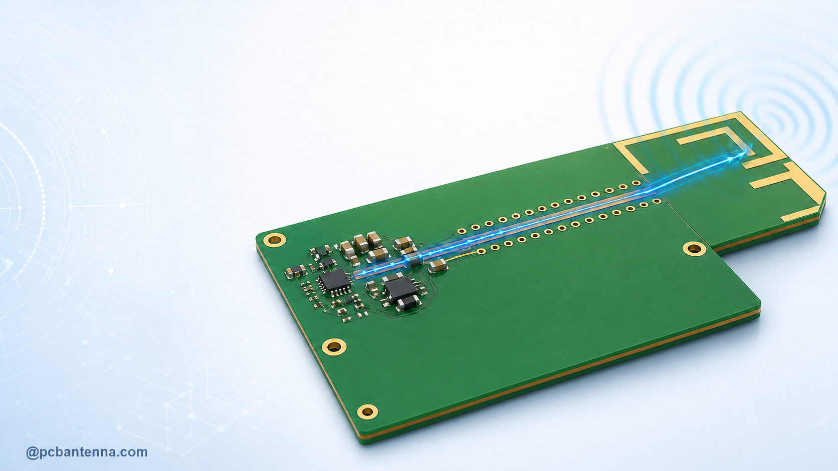
A 50-ohm antenna feed line is not just a trace drawn between the radio and the antenna. At RF frequencies, that trace behaves as a transmission line. Its width, copper thickness, dielectric material, distance to the reference plane, nearby ground copper, vias, bends, and component pads all affect its characteristic impedance and loss.
This guide explains how to design a 50-ohm PCB trace for an antenna feed, when a microstrip or grounded coplanar waveguide makes sense, and how to avoid the layout details that quietly spoil an otherwise good antenna. The target is a repeatable RF path, not a magic trace width copied from another board.
The antenna feed carries RF energy from the radio or matching network to the antenna. If its impedance is controlled and its return path is continuous, it behaves predictably. If the feed passes over a split plane, changes width at random, includes a long stub, or runs through noisy circuitry, it can add reflection, loss, coupling, and unintended matching effects.
For many single-ended RF radios and antennas, 50 ohms is the interface reference used by the transceiver, cable, VNA, and antenna data. That is why a 50-ohm feed is common. It does not mean the antenna itself is permanently 50 ohms; the feed is one part of the complete antenna system. See the antenna impedance guide for the distinction.
A trace does not have one universal impedance based only on its width. For a microstrip, the important inputs include trace width, copper thickness, the dielectric constant of the material, and the distance from the signal layer to the ground reference plane. For grounded coplanar waveguide, the gap to adjacent ground copper and via strategy also matter.
Two boards made from FR-4 can need very different widths for 50 ohms because their stackups differ. A thin dielectric layer between the trace and ground plane generally permits a narrower 50-ohm trace than a thick dielectric layer. Manufacturer stackup data is more useful than a generic FR-4 assumption, especially as frequency rises or tolerance becomes tight.
Analog Devices’ RF layout guidance similarly notes that controlled impedance depends on substrate dielectric constant, trace width, copper thickness, and height above the ground plane. Use the Microstrip Line Calculator for a first estimate, then use the PCB fabricator’s impedance calculator or field-solver data for the actual stackup.
Microstrip places the RF trace on an outer layer with a continuous ground plane directly beneath it. It is simple to route and easy to reason about when the stackup is controlled. The ground plane is the return path, so a split, void, or unexpected cutout under the trace changes the line.
Grounded coplanar waveguide, often abbreviated GCPW, uses ground copper on the same layer beside the signal trace as well as a ground reference below. It can be useful when a narrower line is needed or when the RF path benefits from more confined fields. The side-ground gap and stitching vias are part of the geometry; treating GCPW as an ordinary microstrip in a calculator produces the wrong result.
Choose the topology that matches the radio, antenna reference design, manufacturing capability, and available board layers. Do not switch a supplier’s reference layout from microstrip to GCPW simply because one looks neater. That is an RF redesign and needs calculation, simulation, and measurement.
TI’s reference-design guidance for changing PCB layer thickness shows the practical reason for this discipline: if the stackup changes, trace dimensions must be adjusted to retain equivalent impedance. Copying a 50-ohm width from a 0.8 mm board onto a 1.6 mm board without recalculation is not a safe shortcut.
Keep the feed path as short and direct as the reference layout allows. Avoid unnecessary meanders, long branches, test pads that create stubs, and sharp geometry changes. Gentle bends or properly designed corners are preferable to abrupt discontinuities. A trace that must turn or transition layers can still work well, but the return-current path and impedance transition need deliberate design.
Never route a controlled-impedance feed over a split, slot, or clearance in its reference plane. RF return current wants to follow the signal path closely. When the plane is interrupted, the return takes a larger loop, which can add inductance, radiation, and coupling. Keep the reference plane solid from radio through matching components to the antenna feed unless the antenna design intentionally creates a clearance zone.
For GCPW and RF sections with adjacent top-layer ground, stitching vias connect that copper to the reference plane and help maintain a stable electromagnetic environment. Place them according to the chosen geometry and reference layout. Too few vias can allow side ground to float or form unwanted slot behavior; vias placed inside an antenna keepout can detune the radiator.
If an RF feed changes layers, provide nearby ground-return vias so the signal transition and return transition stay together. A signal via by itself forces the return current to find another path, creating a discontinuity. Keep layer transitions rare; a single clean transition is easier to model and verify than a feed that moves between layers several times.
Place the matching network close to the antenna feed when the antenna reference design calls for it. Keep the interconnect between components short and avoid large pads or branches. At RF, those pads and short traces have inductance and capacitance; they are part of the network rather than invisible wiring.
Use a pi footprint when tuning flexibility is needed, but do not populate components by habit. Measure the actual antenna impedance first, then design the network for the target band. The impedance matching guide covers that process, while the ground-plane guide explains why matching cannot repair every layout problem.
Do not run fast digital clocks, switching nodes, power inductors, or other high-energy traces alongside the RF feed. Parallel routing increases coupling. Keep clearance where possible, cross unrelated layers orthogonally when a crossing is unavoidable, and use the ground structure to shield and control the path. Also avoid routing the feed into the antenna keepout or placing silkscreen and metal features where the antenna vendor prohibits them.
An impedance calculator is an engineering starting point, not a certificate. Fabrication tolerances, copper roughness, actual dielectric properties, solder mask, connectors, components, and surrounding geometry all contribute. Where the feed is critical or long enough to matter electrically, use simulation, a calibrated VNA, or a test coupon to confirm the design.
Measure at a meaningful reference plane and compare the result with the expected S11 and impedance. The HFSS S11 simulation guide describes model setup and correlation; real hardware measurement is still the final check for a product antenna path.
A 50-ohm antenna feed is a controlled transmission-line system, not a line-width annotation. Start from the finished stackup, choose the right topology, protect the return path, keep the route short and quiet, and verify the result when it matters. For a broader layout foundation, read PCB Antenna Design Basics. For design review or RF layout support, explore our antenna design services or contact PCB Antenna.