Get "10 RF Design Principles Every Engineer Should Know" Free
Learn practical principles for better RF circuits, PCB layouts, simulations, measurements, and troubleshooting.

A practical antenna impedance guide covering resistance, reactance, resonance, 50-ohm references, VNA measurement, simulation, and product integration.

Antenna impedance is one of the first RF numbers engineers meet and one of the easiest to oversimplify. It is tempting to ask, “Is this antenna 50 ohms?” The more useful question is, “What is its complex impedance at the frequencies, board condition, enclosure state, and measurement plane that matter to this product?”
This practical guide explains antenna impedance in plain engineering terms: resistance and reactance, resonance, 50-ohm references, S11 and VSWR, measurement, simulation, and what to change when a compact PCB antenna is not behaving as expected. It complements our matching-network guide by focusing first on the antenna quantity you need to understand before selecting components.
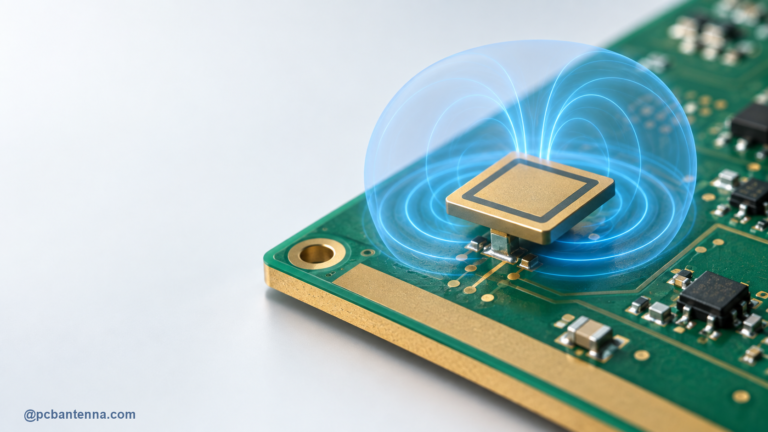
Impedance is the opposition a circuit presents to alternating current at a particular frequency. It is written as Z = R + jX. The real part, R, is resistance. For an antenna, it includes radiation resistance, which represents power carried away as electromagnetic radiation, as well as conductor, dielectric, and other losses. The imaginary part, X, is reactance: energy stored temporarily in electric or magnetic fields.
Positive reactance is commonly described as inductive and negative reactance as capacitive. At a frequency where the inductive and capacitive effects cancel, the input reactance may be near zero. That is often called resonance, but resonance alone does not guarantee a good interface match, high efficiency, or a desirable radiation pattern. The remaining resistance still needs to be considered relative to the system reference.
Many RF radios, coaxial cables, connectors, test instruments, and single-ended PCB feeds use a 50-ohm reference impedance. That makes 50 ohms convenient for interfacing and measurement. It does not mean every antenna naturally presents 50 + j0 ohms. In fact, a small embedded antenna rarely holds one fixed impedance over an entire operating band.
Texas Instruments’ Antenna Impedance Measurement and Matching application note makes this distinction clearly: high-frequency traces and antenna structures have frequency-dependent reactance, and the physical conditions of the end device affect the result. The correct design task is to measure or predict the antenna impedance, then transform it toward the required system impedance over the useful frequency range.
Every antenna impedance is a function of frequency. On a VNA or simulation sweep, the impedance moves through different resistance and reactance values as frequency changes. Near one resonance the antenna may be capacitive below the target frequency and inductive above it, or the opposite depending on the antenna and reference plane. A multiband antenna can show several distinct resonant regions.
This is why a single impedance number without a frequency is incomplete. A datasheet value, a Smith chart marker, or a match component value only makes sense when the stated frequency, bandwidth, board configuration, and reference impedance are known. Use the Wavelength Calculator to relate the operating frequency to physical dimensions; as frequency rises, ordinary PCB dimensions become a larger electrical part of the design.
For a PCB antenna, the copper trace is only one part of the system. The board ground plane, board outline, feed route, antenna position, nearby components, shield cans, battery, display, enclosure plastic, screws, cable, mounting surface, and a user’s hand can all change the impedance. Some effects shift resonance; others add loss, change the radiation pattern, or create an unintended current path.
That is why an antenna should be measured close to its final configuration. A bare prototype is useful for establishing a baseline, but it does not replace a measurement with the intended housing and major nearby objects. The PCB antenna ground-plane guide covers the ground and keepout details that are especially likely to shift impedance in compact products.
Impedance is the underlying complex quantity. S11, return loss, and VSWR are common ways to describe how that impedance compares with a chosen reference. For a one-port device, the reflection coefficient is Gamma = (Z – Z0) / (Z + Z0). A point equal to Z0 gives zero reflection in the ideal model. S11 is often shown in dB as 20 log10 of the magnitude of that reflection coefficient.
These values are related, but they answer slightly different questions. A Smith chart shows the impedance movement and makes reactance visible. An S11 plot makes the frequency response easy to compare. VSWR is often used as a simple match specification. Our S11 and return loss guide explains the relationships and the limits of using any one value by itself.
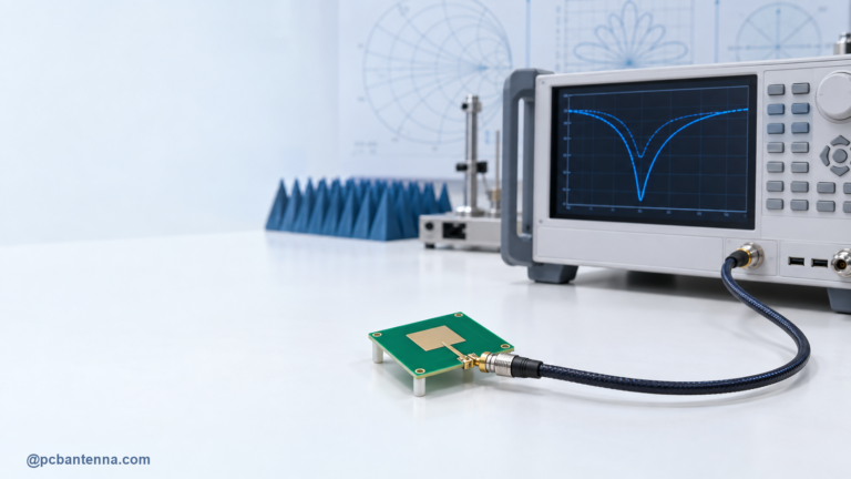
A vector network analyzer can measure S11 and display the antenna impedance across frequency. The most important practical step is choosing the calibration plane. Calibrate the VNA so the reference plane is as close as practical to the antenna feed, including the cables, adapters, and fixture that will remain in the measurement path. If the calibration plane is left at the instrument while a long cable is added later, the cable becomes part of the result.
Use good RF connectors and a mechanically stable fixture. Keep unnecessary wires and tools away from the antenna. If the product will use a battery, enclosure, or cable, measure both the bare board and the final assembly so the differences are visible. TI recommends SOL calibration with the intervening cables and adapters included when characterizing the antenna; the point is to compensate the test path rather than mistaking it for the antenna.
Full-wave simulation can predict impedance, current distribution, and the effect of layout changes before fabrication. The model needs the actual board outline, copper, feed, ground structure, substrate, and relevant enclosure or nearby metal. An inaccurate ground plane or a port that does not represent the physical feed can create an attractive S11 curve that does not correlate with hardware.
Use simulation first to compare controlled changes: board length, antenna location, clearance, matching footprint, or enclosure distance. Then measure a prototype and use the differences to improve the model. The HFSS S11 simulation guide covers ports, boundaries, sweeps, meshing, and correlation in more detail.
A Smith chart plots normalized impedance relative to the selected reference. On a 50-ohm impedance chart, the centre corresponds to 50 + j0 ohms. The horizontal line is purely resistive; the upper and lower halves show positive and negative reactance. A sweep traces a path across the chart as frequency changes, making it easier to see whether the antenna is mainly capacitive or inductive around the band and how quickly it changes.
The chart is not just for drawing component values. It helps separate two questions: does the antenna geometry need to change, or is there a sensible impedance transformation to make at the feed? If the path is far from the target because the antenna is badly affected by a small ground plane or nearby metal, a complex matching network may be a fragile fix. Read our impedance matching and Smith chart guide for the next stage of the workflow.
When resonance is far from the desired band, start by checking the antenna geometry, electrical length, ground plane, and clearance before reaching for a network. For many resonant antennas, physical length is strongly related to resonance; changing it shifts the response. The exact direction and amount depend on the topology and environment, so use a controlled simulation or measurement instead of making a large blind edit.
Once the radiating structure is close to the intended band, a compact matching network can remove residual reactance and transform the resistance toward the feed reference. This division of labor generally gives a more stable result than using components to compensate for a fundamentally unsuitable layout. The inverted-F antenna guide provides a concrete PCB example.
A well-matched antenna accepts power efficiently at its input, but that does not guarantee all accepted power becomes useful radiation. Conductor and dielectric losses, body loading, enclosure absorption, and an unfavorable pattern can still limit link performance. After impedance tuning, check efficiency, realized gain, polarization, and the far field. The antenna gain guide and radiation pattern guide are useful follow-ons.
Antenna impedance is a frequency-dependent property of the entire antenna system, not just the visible radiator. Measure it at the right plane, model the real board and enclosure, fix geometry and integration first, then use matching components as a controlled refinement. For initial transmission-line and link calculations, use the PCB Antenna calculator collection. For an antenna review, impedance measurement plan, or product-level validation, explore our antenna design services or contact PCB Antenna.