
Get "10 RF Design Principles Every Engineer Should Know" Free
Learn practical principles for better RF circuits, PCB layouts, simulations, measurements, and troubleshooting.

Learn how to define a PCB antenna keepout area, protect it from copper and components, route the RF feed correctly, and validate wireless performance.

A PCB antenna can look perfectly reasonable in a layout review and still perform poorly once the board is assembled. One of the most common reasons is not the antenna trace itself, but the space around it. That space is usually called the antenna keepout area: a deliberately controlled region where copper, routing, components, hardware, and enclosure details are kept away from the radiating part of the design.
It is tempting to treat the keepout as leftover board area. In practice, it is part of the antenna system. Nearby metal and dielectric materials can change the antenna impedance, detune its resonant frequency, reduce efficiency, or reshape the radiation pattern. The exact geometry depends on the antenna type, frequency band, board stackup, enclosure, and manufacturer reference design. That is why a vendor-approved reference layout should always take priority over generic rules.
An antenna radiates by establishing electric and magnetic fields around its conductor. Objects inside those fields become part of the electromagnetic environment, whether you intended that or not. A ground pour below a chip antenna, a signal trace beside an inverted-F antenna, or a battery placed close to a board-edge radiator can all alter the result.
For a printed or chip antenna, the keepout normally protects three things:
Silicon Labs, for example, notes in its PCB antenna guidance that a ground plane directly underneath the antenna region can reduce radiation efficiency. Nordic Semiconductor likewise recommends following its reference layouts closely and documents cases where inner-layer clearance reduces unwanted stray capacitance around RF circuitry. These are not conflicting rules; they are reminders that the correct clearance is antenna- and layout-specific.
Start by identifying the antenna keepout on every copper layer, not only the top layer. Unless the antenna data sheet says otherwise, avoid placing the following inside that zone:
Do not assume that a small object is harmless. At RF, a short trace, a via field, or a nearby ground island can create coupling paths that are not obvious in a normal PCB view. The safest workflow is to define the keepout as a layer-aware design rule early, lock it visually in the PCB tool, and include it in every mechanical review.
A useful distinction prevents many layout mistakes: the antenna radiator and its RF feed do not follow the same ground rules. The radiator may need clearance underneath it, while the 50-ohm feed line generally needs a well-defined reference plane to preserve its impedance. Removing ground beneath the entire RF route without checking the reference design can make the feed less predictable.
Keep the route from the transceiver or matching network to the antenna short, direct, and free of unnecessary bends. Use a controlled-impedance geometry that matches the actual stackup, and avoid passing the feed near noisy digital clocks, switching nodes, or connectors. Our guide to 50-ohm PCB trace design for antenna feed lines explains why width alone is not enough to guarantee a 50-ohm result.
Many common 2.4 GHz PCB and chip antenna reference layouts place the radiator at a board edge or corner. This gives the antenna a clearer path into free space and reduces coupling to the rest of the board. If the selected antenna shows that placement in its documentation, preserve it rather than moving the part inward merely to simplify placement.
The board ground plane is also part of the system. A ground plane that is too small, too fragmented, or shaped differently from the approved reference can change tuning and radiation behavior. Before changing the board outline, review the antenna vendor’s suggested ground dimensions and copper boundaries. For a broader discussion, see PCB antenna ground-plane rules that actually matter.
A keepout that exists only in the RF engineer’s first layout revision is not enough. It needs to survive schematic updates, mechanical changes, manufacturing edits, and enclosure design. A practical review checklist looks like this:
Ground stitching can be useful along the edge of the main RF ground area when the reference layout calls for it, but those vias belong outside the radiator keepout. Their purpose is to maintain a low-inductance ground boundary, not to fill the antenna clearance with metal. Keep the same discipline with copper pour updates: a late automatic refill should never silently invade the protected area.
Even when an antenna is advertised as 50 ohms, final performance can change with the board, enclosure, and nearby materials. Leave space for the recommended matching network near the antenna feed and follow the component order in the reference design. This gives you a controlled place to tune the design after measurement instead of cutting traces and improvising components later.
For a printed monopole, the geometry, board edge, and ground area are particularly important. The principles in our printed monopole antenna design for 2.4 GHz devices article are a good companion when you are choosing the antenna style as well as protecting its keepout.
A layout review reduces risk, but it does not replace measurement. Measure return loss or S11 on the assembled board, then repeat the test with the intended enclosure, battery, and major cables in place. If you have simulation capability, use it to compare layout revisions and examine how nearby objects affect the result. Our guides to setting up S11 simulation in HFSS and far-field radiation patterns for PCB antennas can help connect the layout decision to measurable RF behavior.
A carefully protected keepout area is one of the lowest-cost ways to improve antenna repeatability. It prevents late-stage surprises, makes tuning more meaningful, and gives the selected antenna a fair chance to behave like its data sheet says it should. For calculator tools and related design resources, visit the RF and antenna calculators page. For a design review or application-specific support, contact PCB Antenna.



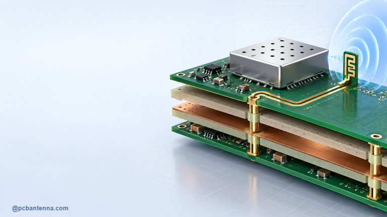


[…] Reference layouts commonly place board antennas at an edge or corner and protect their no-copper zone on all layers. The exact dimension belongs to the selected antenna data sheet. The general workflow is covered in antenna keepout area layout rules. […]
[…] Do not assume the same rule applies under the radiating part of the antenna. Some antenna types need a defined no-copper region below the radiator, while the feed line needs a solid reference plane. Follow the selected antenna’s documentation layer by layer. This distinction is central to antenna keepout design. […]