Get "10 RF Design Principles Every Engineer Should Know" Free
Learn practical principles for better RF circuits, PCB layouts, simulations, measurements, and troubleshooting.

A practical chip antenna integration guide covering reference layouts, keepouts, RF feeds, matching networks, enclosures, and final-product validation.
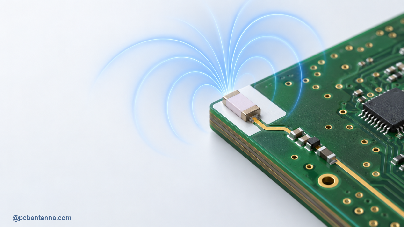
A chip antenna data sheet is not a guarantee of finished-product performance. It is a controlled starting point. The advertised result was obtained with a particular footprint, board size, ground pattern, clearance, feed, matching network, and measurement method. Change any of those things, and the antenna may still work, but it may not behave like the reference chart.
This does not make chip antennas unpredictable. It means they need to be integrated as RF subsystems. A careful design can use the data sheet as a strong head start, then verify the actual PCB and enclosure with measurement.
Start with the supplier’s full layout package, not only the land pattern. Look for the specified board layers, ground dimensions, antenna edge position, keepout, RF feed geometry, matching components, component orientation, and test setup. Check whether the result assumes a particular board thickness or dielectric material.
It is common to find a tiny antenna footprint beside a much larger recommended copper clearance. That clearance is not wasted area. It lets the antenna interact with the intended ground plane and free space. If the product cannot preserve the required clearance, choose a different antenna or change the board architecture before routing becomes difficult.
The board ground plane often acts as a counterpoise for compact antennas. Its size and shape affect impedance and radiation. Traces, vias, copper islands, screws, and nearby components can couple into the radiating region. The same chip on two different boards can therefore show different S11 and range results.
Set up a keepout rule across every relevant layer. In its RF layout guidance, Infineon explicitly recommends keeping components, planes, mounting screws, and traces out of an antenna keepout on all layers. Use that as a discipline, while following the exact dimensions in the selected antenna documentation. Our antenna keepout article explains the review process.
Place the matching network where the reference design places it and keep the route short. Use the correct controlled-impedance geometry for the actual stackup. Extra trace length is not electrically free at RF. It contributes inductance, capacitance, and phase shift that were not included in the nominal component values.
Include component options for tuning unless the supplier explicitly says otherwise. A practical first revision often provides the recommended matching pads and a way to populate, depopulate, or adjust components after VNA measurement. That is far more controlled than cutting a trace after the enclosure has already been built.
Plastic walls, battery packs, flex cables, shields, and nearby metal can shift the resonance or change the radiation pattern. Measure the bare PCB for a baseline, but make the release decision with a final-like assembly. If possible, test the typical user orientation and mounting condition too. A device that passes on an open bench can behave differently in a hand, cabinet, vehicle, or metal-adjacent installation.
If the antenna shifts once the enclosure is installed, do not immediately blame the chip component. Compare the mechanical configuration, board clearance, ground plane, feed, and matching network first. The antenna detuning guide gives a step-by-step comparison approach.
Chip antenna integration becomes much more predictable when the reference design is respected and the final product is measured. For 50-ohm feed details, review 50-ohm PCB trace design. For project-specific review, contact PCB Antenna.