Get "10 RF Design Principles Every Engineer Should Know" Free
Learn practical principles for better RF circuits, PCB layouts, simulations, measurements, and troubleshooting.

Set up, plot, and validate HFSS far-field radiation patterns for PCB antennas with practical guidance on spheres, coordinates, polarization, and gain.
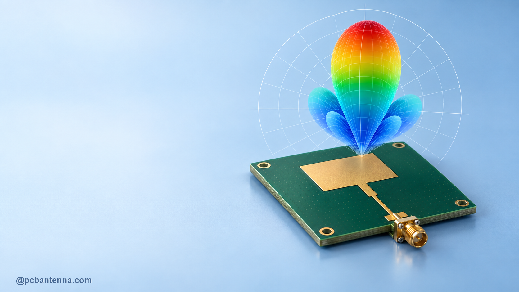
A PCB antenna can have an acceptable S11 curve and still radiate in an unhelpful direction. That is why a far-field radiation pattern belongs in the normal HFSS workflow, not at the very end as a decorative 3D plot. The pattern shows where the simulated energy is going, where the nulls are, and whether the antenna still behaves sensibly after the board, ground plane, and nearby product geometry are included.
This guide walks through an HFSS far-field radiation pattern setup for PCB antennas. It focuses on the decisions that usually matter most: preparing a trustworthy model, creating the far-field observation sphere, choosing coordinates and polarization, making useful 2D and 3D reports, and checking whether the result deserves confidence.
Far-field data describes the antenna response away from the radiating structure. In HFSS, an infinite sphere can be used as the observation domain, then reports can evaluate quantities across chosen theta and phi angles. That lets you inspect a full 3D shape or a single cut through the pattern. Ansys documents that far-field results require saved fields in the solution and sweep setup, along with a far-field sphere surrounding the radiating object.
For a PCB antenna, the answer is rarely a perfect donut or a neat lobe. The board ground often participates in radiation. A display, battery, shield can, cable, or enclosure can bend the pattern further. The useful question is not “does the plot look impressive?” but “does it provide enough coverage in the orientations and frequencies this product needs?” Our radiation-pattern guide is a handy primer on lobes, nulls, and common plot language.
Before adding a far-field request, make sure the model represents the physical state you want to predict. Include the antenna copper, board outline, substrate stackup, feed, matching network or its footprint, and the relevant ground plane. If the final product has a connector, battery, cable, metal bracket, or enclosure close to the antenna, add those parts in a controlled second stage. Their effect may be the actual engineering question.
Also make sure the excitation and S11 result are credible first. A radiation pattern based on an incorrect port, missing return path, or badly placed boundary can be perfectly smooth and completely misleading. Use the HFSS S11 setup guide to check the feed and solution setup, and compare the board treatment with these PCB antenna ground-plane rules.
Your antenna needs an air region around it so HFSS can solve the fields leaving the board. Apply the boundary method appropriate for your design and solver workflow, following the current HFSS documentation. The practical aim is simple: keep the artificial boundary far enough away that it is not controlling the answer, while avoiding a model so large that it becomes needlessly expensive to solve.
Do not borrow an air-box size blindly from a different antenna, frequency, or tutorial. Run a small sensitivity check when the result matters. If moving the boundary or refining the solution changes the key gain or pattern shape substantially, the simulation is telling you to investigate the setup before using the plot for a design decision.
Far-field post-processing depends on field data being available for the solved frequencies. Check the solution and sweep settings before launching a long run, especially when you intend to review several operating bands. Choose solution frequencies that make sense for the antenna, then make sure the sweep covers the full target range with enough resolution to reveal shifts, narrow modes, and unexpected resonances.
Antenna patterns can change noticeably across a band. Do not assume that the pattern at the deepest S11 dip represents every channel or operating frequency. For a multiband device, choose a small set of frequencies that reflect the lower edge, center, and upper edge of each important band, then compare the same cuts and metrics at each one.
In standard HFSS, use the Radiation menu to insert a far-field setup with an infinite sphere. The sphere surrounds the radiating structure and provides the angular observation domain for reports. Ansys describes this workflow as defining the sphere sampling, then selecting the sphere from the report dialog when plotting far-field values.
Give the setup a clear name when a project contains more than one configuration, such as FF_FreeSpace or FF_Enclosure. It makes later comparison much easier. Define theta and phi start, stop, and step values with the report you need in mind. A coarse grid is enough for a quick orientation check. A finer grid may be appropriate when locating a narrow null, peak direction, or polarization feature. More points cost post-processing time, so use resolution intentionally.
Coordinate choices are an easy way to create confusion. The default spherical system commonly uses theta and phi, but the important part is how those angles relate to the physical product. Decide which board edge, display direction, or device orientation should be your reference. If the default axes do not make that obvious, create a named coordinate system tied to the board or product.
Write the orientation down in the project notes and in exported plots. A broadside lobe in one coordinate system can look like an end-fire lobe in another. For a handheld or wall-mounted product, a pattern without a clear “up,” “front,” or “board normal” reference is difficult for another engineer to review or compare with chamber data.
Polarization is not just a report setting. It affects how you judge a link between the antenna and a receiver. Use the far-field setup to select the desired coordinate system and polarization basis, then inspect co-polar and cross-polar responses when the application needs them. A general-purpose IoT antenna may be judged mainly on practical coverage and robustness to orientation, while a directional link may have a much stricter polarization requirement.
Be consistent from simulation to measurement. If a chamber test calls one axis vertical, define the simulated comparison cut so it means the same thing. Otherwise a real disagreement can hide behind a naming mismatch. For a wider look at efficiency, gain, and what the numbers mean together, see our antenna gain guide.
Start with a 3D polar plot. It gives a fast view of the dominant lobes and deep nulls, and it can reveal a surprising tilt caused by the board or nearby hardware. HFSS supports creating far-field reports from the Results area after the sphere is available. Use the same frequency and source conditions throughout the comparison so one pattern is not accidentally normalized differently from another.
Then create 2D cuts through the planes that matter. A common approach is to hold phi constant and sweep theta, then repeat for a second orthogonal phi plane. For a product antenna, include a cut that corresponds to the device’s most important user orientation. Label every plot with the frequency, quantity, cut plane, coordinate system, and normalization choice.
There is no single best quantity. Directivity shows the shape created by the radiation distribution without including mismatch and loss. Gain includes losses. Realized gain also includes the effect of input mismatch, so it is often the more practical antenna-level quantity when comparing delivered system performance. Inspect the S11 and efficiency alongside it so the plotted value has context rather than becoming an isolated headline number.
Normalize only when it helps answer a shape question. Normalized plots make lobe and null comparison easy, but they can conceal an important drop in absolute performance. Keep at least one absolute-gain or realized-gain view for each important design revision.
First, review adaptive convergence and current distribution. The strongest current should have a physical explanation. If unexpected current appears on a cable, shield, fixture, or board feature, investigate it before treating the far-field plot as the antenna’s intrinsic behavior. Run a geometry, boundary, or mesh sensitivity study when a small model change moves the lobe or gain more than your design margin allows.
Next, compare simulation with hardware when a prototype is available. Use a repeatable orientation and test configuration. A mismatch between chamber data and HFSS can come from material data, cable routing, missing mechanical parts, an incomplete enclosure model, alignment differences, or test-fixture coupling. The goal is not to force one curve or plot to match. The goal is to find the physical detail that explains the difference and then test whether the updated model predicts the next change.
A far-field radiation pattern in HFSS becomes useful when it is tied to a real engineering decision: board placement, enclosure choice, orientation coverage, tuning, or a comparison against measured hardware. For the complete simulation flow, read the HFSS antenna simulation workflow. If you need help reviewing a model, optimizing coverage, or correlating a PCB antenna with measurements, see our antenna design services or contact PCB Antenna.