Get "10 RF Design Principles Every Engineer Should Know" Free
Learn practical principles for better RF circuits, PCB layouts, simulations, measurements, and troubleshooting.

A practical HFSS S11 simulation guide for PCB antennas covering geometry, materials, ports, boundaries, meshing, sweeps, interpretation, and validation.
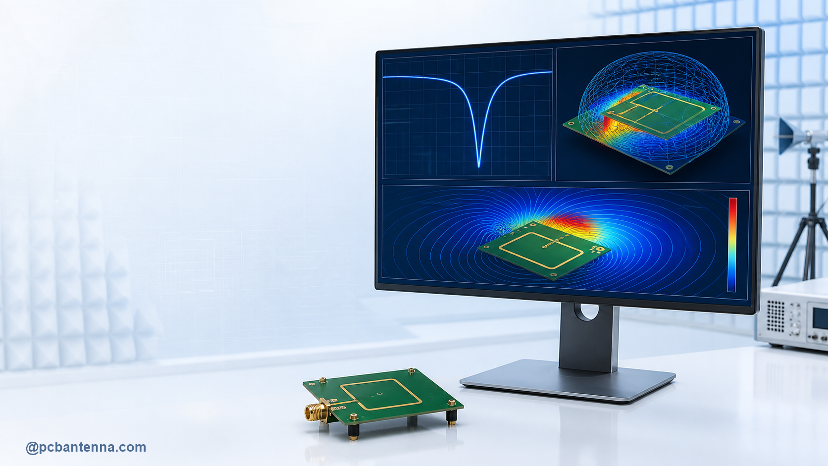
An S11 simulation is often the first useful check in a PCB antenna project. It shows how well the antenna input is matched to the feed system across frequency, helps you spot the resonance region, and gives you a controlled way to compare changes before hardware is built. It is also easy to make a simulation look better than reality by leaving out the ground plane, enclosure, connector, or a correct excitation model.
This practical HFSS guide explains how to set up S11 simulation for a PCB antenna, what each modelling choice is doing, and how to turn a nice curve into a result you can trust. The workflow applies to common trace, chip, inverted-F, patch, and module antenna projects, with the part-specific reference layout always taking priority.
S11 is the input reflection coefficient of port 1. In plain terms, it describes how much of the incident RF signal is reflected back toward the source because the antenna input does not match the reference impedance. It is often plotted in decibels as 20 log10|S11|. A value of -10 dB corresponds to about 10% reflected power; a more negative value means less reflected power at that frequency.
That makes S11 valuable, but it is not a complete antenna scorecard. A good S11 curve does not prove high radiation efficiency, good gain, or a useful radiation pattern. It only says something about the input match in the simulated configuration. Use it alongside current distribution, efficiency, realized gain, and far-field results. Our S11 and return loss guide explains the measurement in more detail.
Start with a clear target. Are you checking a reference antenna before integrating it? Tuning a matching network? Comparing board sizes? Investigating why a final product shifted frequency? The purpose determines how much geometry belongs in the model. A bare-board simulation is useful for understanding the antenna, but it cannot predict a product that will be mounted beside a battery, display, cable, or metal enclosure.
Set the frequency range around the intended operating band with enough margin to see the resonance move. For a wideband or multiband antenna, include every important band rather than relying on a narrow sweep around a single expected dip. Record the stackup, dielectric constant, substrate thickness, copper thickness, and intended reference impedance before modelling. These are inputs, not cosmetic settings.
Model the antenna trace, feed line, matching components or footprints, ground plane, board outline, and relevant layers. The ground plane deserves the same attention as the visible antenna copper. For many compact PCB antennas, changing ground length, adding a slot, or moving the antenna away from the board edge shifts the input impedance and radiation behavior.
Use dimensions from the layout database or manufacturer drawing rather than approximating from a screenshot. Include vias that connect RF ground regions, especially around a shorting arm or feed return. If a component is not yet selected, model a sensible placeholder only when you clearly document the assumption. A mismatched board outline with a perfectly drawn antenna trace is still the wrong antenna model.
The PCB antenna ground-plane guide is a helpful companion here: it explains why the keepout and ground structure must both match the intended layout. For a trace or inverted-F antenna, also compare your geometry to the inverted-F PCB layout guide.
Assign the substrate dielectric properties and thickness for the actual PCB construction. A generic FR-4 value can be acceptable for an early sensitivity study, but material properties vary with construction and frequency, and a final design should use the best available stackup data. Use finite conductivity or an appropriate conductor model for copper when the loss mechanism matters to the question being asked.
Include major nearby dielectric or conductive objects when they are part of the final product. A plastic housing can shift tuning; a battery or shield can can block or detune the antenna; a USB cable may become part of the radiating environment. Add complexity in stages so you can see which object caused a change rather than putting every uncertain object into the first solve.
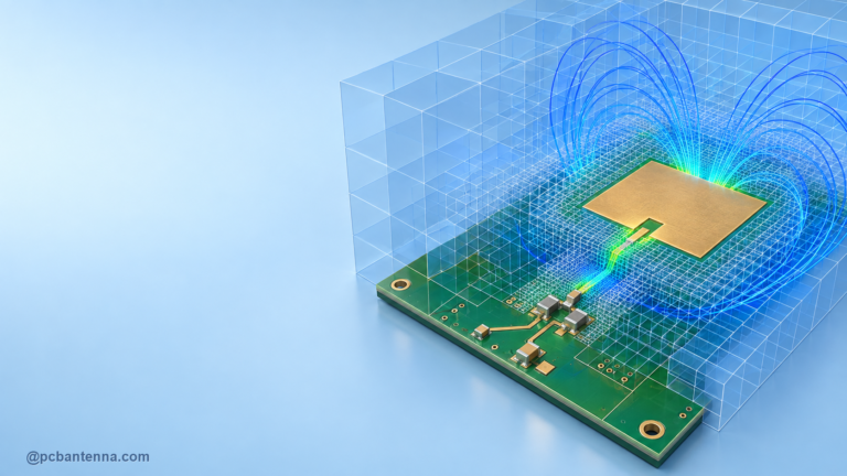
An antenna needs a surrounding air volume so the solver can represent fields extending away from the board. Enclose the structure in an air region large enough for the boundary treatment and frequency range you are using, then assign the appropriate radiation or absorbing boundary according to the HFSS workflow and solver documentation. The key idea is to avoid placing the simulation boundary so close that it changes the antenna response.
Keep this setup physically meaningful. A tiny air box may solve quickly but can create a result that does not represent the antenna in free space. Conversely, an unnecessarily large model can waste time and memory. Start with documented HFSS guidance, then use convergence and sensitivity checks to confirm the boundary choice is not driving the S11 result.
The port defines how energy enters the model, so it must represent the physical feed. A lumped port can be suitable across a short, clearly defined gap or feed connection. A wave port is often used when the feed reaches a model boundary and its transmission-line modes need to be represented. The best choice depends on the antenna, connector, line geometry, and the HFSS setup being used; do not select a port merely because it appeared in a different tutorial.
Check port orientation, integration line, terminal assignment where applicable, and reference impedance. Make sure the port bridges the intended signal and ground conductors rather than exciting a floating piece of copper. A port that is geometrically convenient but physically wrong can produce a smooth S11 curve that has nothing to do with the manufactured board.
Choose a solution frequency near the most important resonance or within the band where the geometry needs the strongest mesh accuracy. Then create a sweep that covers the intended operating region plus margin on both sides. Use enough sample points or an appropriate adaptive/interpolating sweep method to see narrow resonances rather than accidentally stepping over them.
For an antenna intended to cover several separated bands, consider whether one setup and sweep are giving you enough confidence across all of them. It is often useful to examine current distribution and fields at each important frequency, not only at the deepest S11 dip. A deep dip at an unintended frequency is a clue, not a success condition.
HFSS uses adaptive meshing to refine regions that need more field resolution. Pay attention to thin feed traces, narrow antenna gaps, shorting paths, matching components, and regions where current crowds. The Ansys HFSS product overview describes the software as a full-wave 3D EM tool with automatic adaptive meshing; that capability is useful only when you review whether the result has converged for the quantity you care about.
Do not trust the first curve because it looks smooth. Compare adaptive passes, inspect mesh refinement around critical geometry, and rerun a sensitivity check if a small change in mesh settings moves the resonance noticeably. If the model is large, simplify noncritical features first rather than reducing accuracy at the feed or antenna.
After the solve, identify the resonance locations, bandwidth over your chosen match criterion, and any unexpected modes. Compare the curve with input impedance. A resistance near the system reference and a small reactance around the target frequency are typically consistent with a good match, but the full interpretation depends on the antenna and matching network.
Then check surface current and fields at meaningful frequencies. Current flowing on the intended antenna and ground structure is reassuring; a strong current path on a cable, shield, or accidental metal feature can explain surprising behavior. Generate far-field plots and realized gain once the input match is credible. The radiation pattern guide explains what to look for beyond the S11 graph.
Simulation is most valuable when it shortens the path to a measured result. Build a representative prototype, measure S11 with a properly calibrated VNA and appropriate fixture, and compare it with the model. If the curve shifts, inspect the usual suspects: substrate data, board outline, connector launch, cable handling, populated components, enclosure parts, and dimensional tolerances.
Use the gap between measurement and simulation as information. Do not simply retune the model until it matches one measurement. Find the missing or inaccurate physical detail, update the model, and confirm the revised model predicts the next controlled change. That is how a one-off simulation becomes a reliable design tool.
HFSS can provide a powerful view into the S11 behavior of a PCB antenna, but the model is only as useful as the assumptions behind it. For the broader process, see the HFSS antenna simulation workflow. For help with a model, antenna tuning, or measurement correlation, explore our antenna design services or contact PCB Antenna.