Get "10 RF Design Principles Every Engineer Should Know" Free
Learn practical principles for better RF circuits, PCB layouts, simulations, measurements, and troubleshooting.

A practical meandered antenna design guide for small IoT devices covering layout, ground planes, keepouts, matching, bandwidth, and validation.
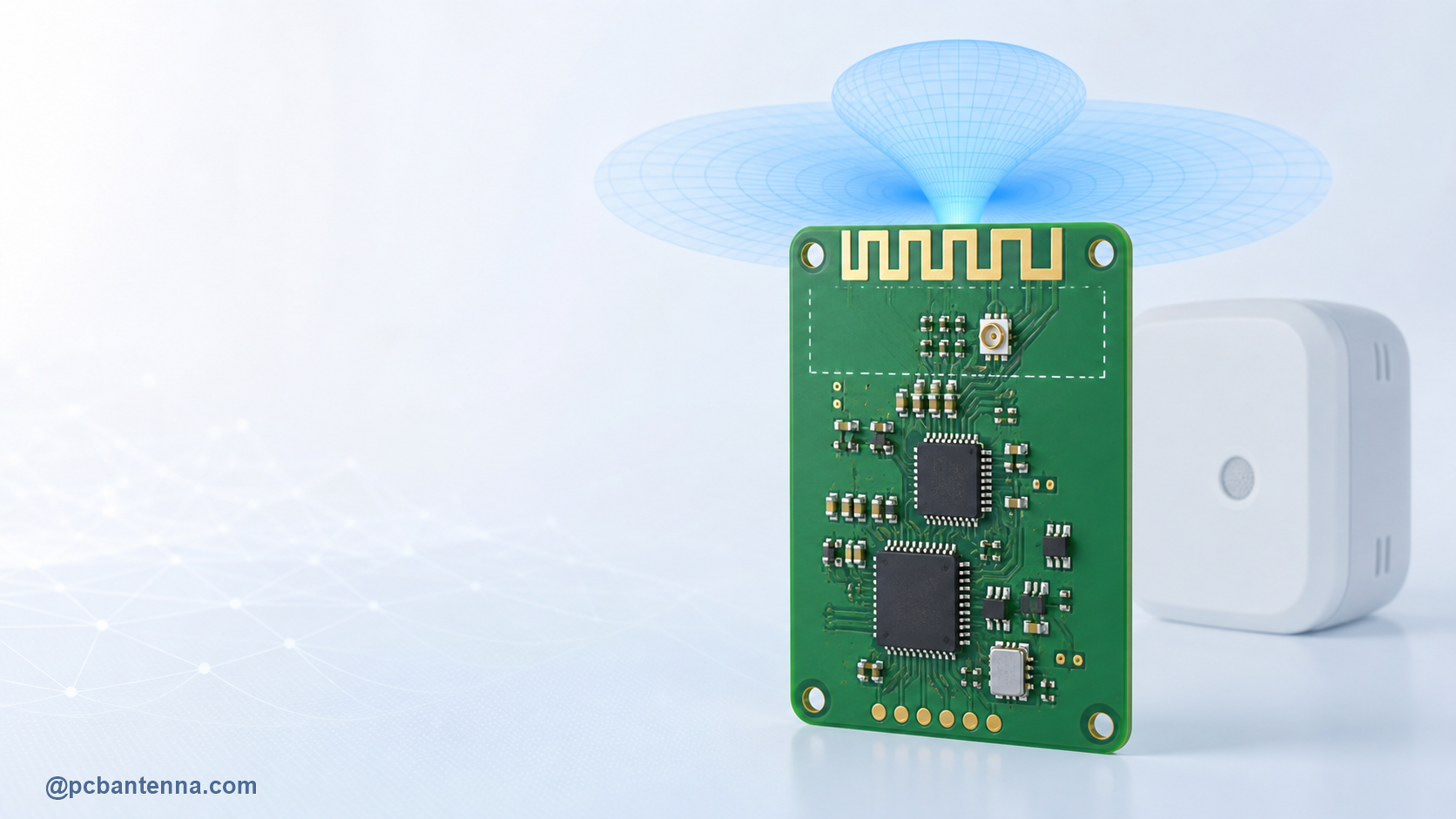
A meandered antenna is a practical answer to a very common IoT problem: the electrical length needed for the radio band is larger than the space available on the PCB. By folding a conductor into a compact path, a designer can fit a resonant structure into a small outline. The saved area is real, but so are the trade-offs. A compact meandered antenna can be more sensitive to ground-plane changes, nearby objects, bandwidth limits, and tuning than a larger layout.
This guide explains how meandered antennas work, when they make sense for small IoT devices, what layout rules matter most, and how to validate them in the final product. It is not a promise that one trace shape works everywhere; the exact reference design, board, and enclosure still decide the outcome.
A meandered antenna routes a conductor back and forth instead of using one straight radiating arm. The folded path increases electrical length within a smaller physical footprint. Meandered monopoles and meandered inverted-F antennas are common forms in compact Bluetooth, Zigbee, Wi-Fi, and sub-GHz IoT designs.
The shape alone does not make an antenna. The feed location, any shorting connection, clearance area, ground plane, board edge, and nearby material all influence the impedance and pattern. TI’s AN043 meandered inverted-F reference is a useful example: it presents a small 2.4 GHz PCB antenna for constrained space while treating matching and board implementation as part of the design.
Small sensors, trackers, plugs, tags, and battery-powered devices often cannot spare a long straight antenna region. A meandered trace can reduce the required edge length and avoid the cost and assembly of an external antenna. It can also be manufactured as part of the PCB, which keeps the RF path short and repeatable when the layout is controlled.
That compactness has a price. Folding the conductor increases interaction between adjacent sections of the trace and can increase stored energy relative to radiated energy. In practice, a smaller antenna may have narrower usable bandwidth, lower efficiency, or greater sensitivity to the enclosure. A meandered design is a good choice when size is genuinely the limiting constraint and the project includes time for tuning and validation.
Before choosing a meandered trace, define the radio band, target range, board space, expected orientations, enclosure, and production tolerance. A larger inverted-F or monopole may be easier to tune and offer more bandwidth if space allows. A chip, flex, or external antenna may be better when the main board is crowded with metal, batteries, or noisy electronics.
For a small single-band device with an understood mechanical environment, a meandered antenna can be an excellent low-cost solution. For multiband coverage, a very small board, or a product held against the body, compare several options early. The antenna that fits the CAD outline is not automatically the antenna that gives the most reliable link.
Many meandered PCB antennas work with the board ground as a counterpoise. That means the ground-plane dimensions and shape are not arbitrary. A smaller ground plane can change impedance, resonance, efficiency, and the radiation pattern. Moving the antenna from the board edge into the middle of a crowded board can also change the result dramatically.
Follow the antenna reference layout first, including its board edge placement and keepout. TI’s DN024 meandering-monopole note recommends copying the antenna dimensions accurately and highlights that ground geometry and nearby objects can require matching adjustment. Our PCB antenna ground-plane guide explains the practical balance between a protected clearance zone and a continuous, useful ground structure.
The clearance around a meandered trace is not empty space waiting for a late PCB feature. It is part of the RF design. Keep copper pours, signal traces, vias, components, shields, battery tabs, cable routes, and metal-backed labels out of the region specified by the reference layout. Check internal layers as carefully as the top layer.
A common failure mode is to copy the antenna shape correctly and then run a ground pour beneath it, place a connector beside it, or route a display cable across the clearance. The antenna may still show a resonance, but it can shift in frequency or lose efficiency. Treat any change inside or near the keepout as a reason to remeasure.
Route the feed from radio to antenna with the intended controlled impedance, a continuous return path, and minimal unnecessary length. Keep digital clocks, switching supplies, and long parallel data traces away from it. A short, clean 50-ohm feed is a common target for many single-ended RF interfaces, but use the radio and antenna documentation as the design authority.
Leave a matching network footprint close to the antenna feed, often in a pi arrangement, even if the first prototype starts with a simple population. The footprint gives you a controlled tuning point after the real board is measured. Do not copy component values from another product: a different ground plane, plastic housing, or battery location can require different values. The matching-network guide explains how to move from measured impedance to a practical network.
Compactness often makes a meandered antenna more narrowband than a larger alternative. That does not make it unsuitable. It simply means the operating band, tolerance, and detuning risk need to be checked honestly. A design that looks good at one centre frequency may not cover the full channel range after plastic, battery, or temperature effects are included.
Do not judge the design only from S11. Check radiation efficiency, realized gain, and the coverage pattern in the intended orientation. The antenna impedance guide explains why the input response moves with the product environment, while the radiation pattern guide shows why a good match does not guarantee useful coverage.
For model setup and correlation, see the HFSS S11 simulation guide. A simulation can show current crowding, detuning, and sensitivity before another PCB spin, but the final housing still needs measurement.
A meandered antenna is a compact RF structure, not a generic decorative trace. It earns its place in a small IoT device when the reference layout, ground plane, keepout, feed, enclosure, and test plan are all treated as one system. Use the PCB Antenna calculator collection for early RF checks, and explore our antenna design services or contact PCB Antenna when the product needs a design review or validation plan.