Get "10 RF Design Principles Every Engineer Should Know" Free
Learn practical principles for better RF circuits, PCB layouts, simulations, measurements, and troubleshooting.

Learn how multilayer PCB stackup, vias, ground planes, shields, and antenna keepouts work together in reliable RF antenna integration.
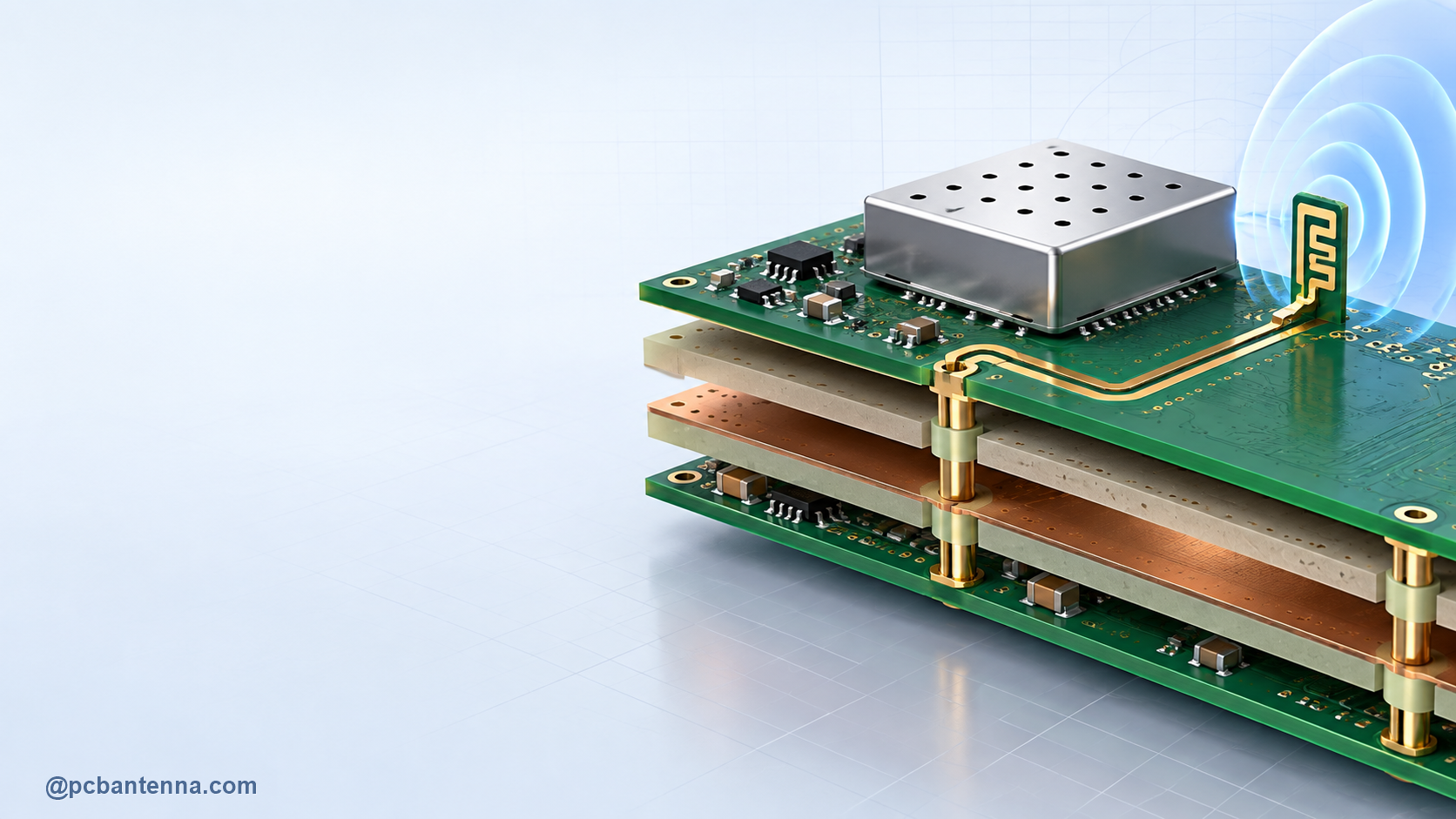
A multilayer PCB gives RF designers valuable tools: a controlled stackup, a dedicated ground plane, shorter return paths, shielding opportunities, and more freedom to separate noisy digital circuitry from the antenna area. It also creates new traps. Inner-layer copper can invade an antenna keepout, a via transition can disturb the feed, and a shield can solve one noise problem while creating an antenna problem nearby.
Choose the layer arrangement with the antenna and feed in mind. A common RF approach places the antenna, RF IC, matching components, and RF route on an outer layer with a close, continuous ground reference plane beneath the controlled feed. The exact stackup depends on fabrication capability, impedance target, component density, and the antenna reference design.
Do not assume the same rule applies under the radiating part of the antenna. Some antenna types need a defined no-copper region below the radiator, while the feed line needs a solid reference plane. Follow the selected antenna’s documentation layer by layer. This distinction is central to antenna keepout design.
A 50-ohm feed is determined by trace width, dielectric thickness, copper geometry, nearby ground, and the actual stackup. Ask the fabricator for the build information, then calculate or simulate the trace geometry. Avoid changing the board layer arrangement after impedance has been signed off without revisiting the feed.
Every via in the RF path adds a discontinuity. Sometimes vias are unavoidable, but they should be deliberate and kept to a minimum. When a transition is required, preserve the return path with nearby ground vias where the reference layout and stackup support that approach. Do not scatter ground vias through the antenna’s protected clearance zone.
RF shields can reduce coupling from noisy digital circuitry, but a shield is also a metal object. Keep it out of the antenna near field and review its effect on the radiation pattern. Use a shield to protect sensitive or noisy circuits, not as a generic fix for an antenna that is badly placed.
Check connector shells, mounting screws, heat spreaders, display brackets, and battery terminals with the same care. Multilayer boards make it easy to focus on internal copper while forgetting the three-dimensional product assembly.
A continuous ground reference under the RF feed helps make impedance predictable and gives current a controlled return path. Splits, slots, or noisy return currents crossing beneath the feed can create unwanted behavior. At the same time, blindly filling every inner layer with copper below the antenna radiator may violate its reference layout. Treat feed and radiator as separate zones with separate ground requirements.
Infineon recommends a multilayer approach for many RF designs and also states that antenna clearance must follow the manufacturer’s ground pattern. The engineering lesson is simple: more layers provide control only when their copper is intentional.
Board stackup is often finalized by the fabrication process after the initial layout has started. If prepreg thickness, copper weight, or layer order changes, revisit the RF feed geometry and antenna assumptions. A narrow trace that was calculated for one dielectric spacing can no longer be assumed to be 50 ohms after the spacing changes. Ask for the final controlled-impedance proposal and document the agreed geometry.
The same discipline applies to optional copper. A plane, shield, or stitching-via pattern that is harmless near digital circuitry may be unacceptable near the radiator. Include antenna layer clearances in fabrication notes and review the final Gerber and assembly data with the antenna reference layout beside them.
For a more detailed feed-line review, see 50-ohm PCB trace design. For help with stackup, RF routing, and antenna integration, contact PCB Antenna.