Get "10 RF Design Principles Every Engineer Should Know" Free
Learn practical principles for better RF circuits, PCB layouts, simulations, measurements, and troubleshooting.

Compare ceramic chip antennas and PCB trace antennas by board area, layout rules, tuning effort, enclosure sensitivity, and production needs.
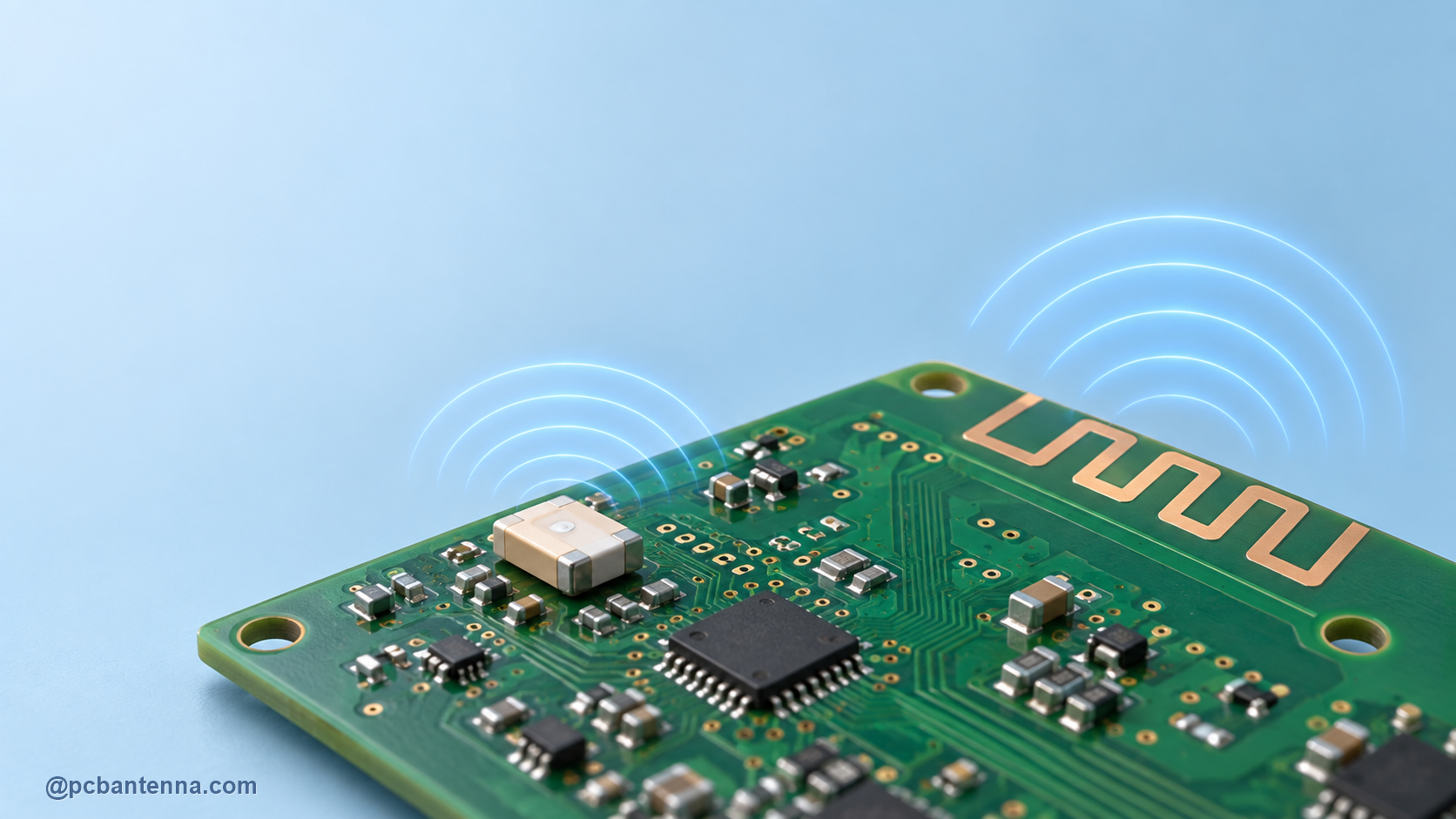
Choosing between a ceramic chip antenna and a PCB trace antenna is not a question of which one is universally better. It is a question of what the product can support. Board size, enclosure, manufacturing tolerance, available RF expertise, target band, cost, and test capacity all influence the right choice.
Both options can work well. Both can also disappoint when their reference layout is treated as optional. The best choice is usually the one that fits the physical product and can be validated with the final board, enclosure, and operating environment.
A ceramic chip antenna is a manufactured RF component with a specified footprint, feed location, clearance area, and usually a reference board. It can reduce the amount of custom antenna geometry on the PCB and can be attractive when the available board area is small. It also makes it easier to carry a known component through procurement and production.
The tradeoff is that the chip antenna still depends on its host PCB. The ground plane, clearance, feed, nearby metal, enclosure, and matching network remain important. A component being pre-characterized does not mean it will perform identically on every board. Treat the data sheet layout as part of the antenna, not merely an assembly drawing.
A PCB trace antenna is created directly from copper on the board. It can avoid the bill-of-material cost of a separate antenna and can be customized for the board shape. It is often a good fit when the board has enough edge area and the team can preserve the required ground relationship and clearance.
The tradeoff is sensitivity. Trace geometry, board thickness, dielectric properties, solder mask, board edge, ground plane size, and nearby product hardware can all affect the result. A copied geometry is only a starting point unless its stackup and surroundings are very similar to the design that validated it.
For either antenna type, study the supplier’s recommended ground plane, clearance on every layer, feed trace, matching topology, and placement relative to the board edge. Texas Instruments notes that many chip antennas require ground clearance on all PCB layers and that tuning should be performed with the final casing assembled. This is a useful reminder that the mounted antenna and the product mechanics must be designed together.
Protect the region with a formal keepout rule. Do not route signals below it, place a screw through it, or let an automatic copper pour refill it late in the project. Start with antenna keepout layout rules before deciding that an antenna needs a different matching network.
Leave the recommended matching footprint on the first revision. Measure the assembled product on a calibrated VNA, compare it with the expected band, and test more than one unit if the product will be produced in volume. If you are using a trace antenna, compare the result with a simulated starting point, but keep the final decision grounded in measurement.
A chip antenna is not automatically easier to tune, and a trace antenna is not automatically less reliable. The reliable path is to select the one whose reference design you can actually honor. A printed monopole antenna may be an excellent option when a board edge and ground plane are available. A chip antenna may be more practical when a validated compact footprint fits the product better.
If the decision is still close, place footprints for two candidates on an early evaluation board, each with its proper keepout and matching network. Test them in the final-like enclosure rather than arguing from a catalog plot. The measurements will show whether board space, range, and tuning margin support the choice.
For layout review or custom antenna support, contact PCB Antenna.