Get "10 RF Design Principles Every Engineer Should Know" Free
Learn practical principles for better RF circuits, PCB layouts, simulations, measurements, and troubleshooting.

Practical PCB antenna ground plane rules for keepouts, RF return paths, feed routing, stitching vias, matching, and final-product validation.
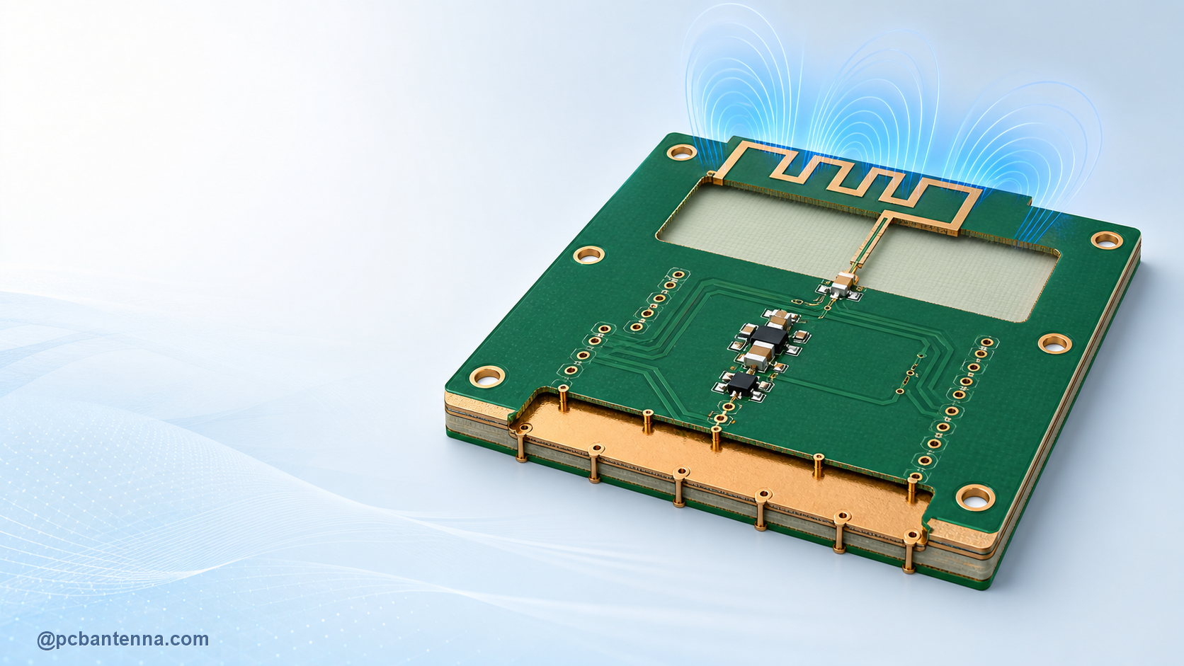
A PCB antenna is not just the visible copper trace at the edge of the board. In many compact designs, the surrounding ground plane, feed line, board edge, and nearby components all contribute to the electrical behavior. That is why an antenna copied from a reference design can look perfect in CAD yet shift frequency, lose efficiency, or develop a weak radiation pattern after a small board change.
The ground-plane rules that actually matter are rarely universal dimensions. They are a set of relationships: where the antenna sits, where copper must be removed, where a continuous return is needed, how the RF feed is routed, and which parts of the final product can disturb the result. This guide turns those relationships into a practical PCB review process.
For many small single-ended antennas, including common monopole-like, inverted-F, and chip antenna implementations, the ground plane is part of the radiating system. Its size and shape affect impedance, efficiency, and the far-field pattern. It is not a passive rectangle that can be resized without consequence. A board made shorter, a large slot added, or a ground connection broken near the feed can change the antenna response even when the antenna trace itself is untouched.
This does not mean that copper should be placed everywhere. A compact PCB antenna often needs a defined clearance region around or below the antenna element so nearby metal does not load it. Silicon Labs’ AN1088 inverted-F antenna note, for example, specifies no ground plane under its antenna section while also using a grounded shorting arm and an adjacent board ground plane. Both statements can be true because they serve different parts of the design.
A supplier reference layout is a tested starting point, not decorative artwork. It normally defines the board thickness, dielectric material, antenna position, keepout, feed width, ground extent, and matching network used to obtain the documented result. Moving a trace by a few millimetres or filling a keepout with copper can be enough to change tuning at 2.4 GHz and above.
Build the first prototype as close as possible to the reference: same antenna orientation, similar board edge, comparable stackup, and the recommended component placement. After you have a measured baseline, make one controlled change at a time. This approach feels slower on day one but is far faster than guessing which of several layout changes caused a poor result.
For the underlying principles, see PCB Antenna Design Basics for Beginners. If your starting point is an inverted-F design, the Inverted-F antenna guide explains the relationship between the radiating arm, shorting path, and ground plane.
When the antenna data sheet calls for a copper keepout, treat it as a three-dimensional keepout. Avoid copper pours, signal traces, vias, components, shields, batteries, and cables in the stated region. Do not forget inner layers. A ground plane on an internal layer can affect an antenna just as surely as copper on the outer layer.
The exact keepout size depends on the antenna type and vendor reference. Some chip antennas need an open region below and around the component; some module antennas are designed to sit at a board edge with clearance only under the radiating end. Do not replace a part-specific drawing with a generic “10 mm rule.” The right rule is the one tested for that antenna, frequency range, substrate, and ground configuration.
A common late-stage mistake is to add a mounting screw, flex cable, debug connector, or metal-backed label inside the keepout after RF tuning is complete. Mechanical additions deserve the same RF review as a change to the antenna trace.
The transmission line between the radio and antenna is part of the RF system. It should have the impedance called for by the design, commonly 50 ohms for a single-ended antenna feed, and it needs a continuous reference plane. A narrow feed that crosses a ground split, passes a large void, or runs alongside a noisy digital clock can introduce loss, unwanted coupling, and a result that is hard to reproduce.
Keep the feed short and direct where possible. Avoid unnecessary bends and stubs. When a change of layer is unavoidable, make the return-current path deliberate with nearby ground vias and follow the stackup-specific routing guidance. The Microstrip Line Calculator is useful for an early width estimate, but it cannot replace a stackup check or a measurement of the finished board.
A continuous ground region near the RF section provides a stable return path and, for many compact antennas, an important counterpoise. Random ground islands and long narrow ground connections are not equivalent to a solid plane. In its antenna guidance, Silicon Labs notes that for monopole-type PCB antennas a sufficiently large continuous ground metallization at the feed region is important to radiation efficiency, matching, and pattern quality.
That does not justify pouring ground through the antenna keepout. Think of the layout as two intentional zones: a quiet clearance zone around the radiating element and a well-connected ground structure where the antenna and feed require a return path. The boundary between them is part of the antenna geometry.
Ground stitching vias can help connect top and inner or bottom ground copper, control the edge of a coplanar or microstrip feed, and reduce discontinuities around the RF section. They must be used where the reference layout calls for them and kept out of the antenna clearance area. A via fence can be helpful next to a feed line, but placing vias under a radiating trace simply because there is empty space can detune the antenna.
Use the vendor layout as the first guide for via location and pitch. If you need to deviate, simulate or measure the change. This is especially important on four-layer boards, where a via pattern can couple the intended feed structure to internal planes in ways that are not obvious in a top-layer view.
Even a good reference antenna may require adjustment in a new product. Board dimensions, plastic housing, nearby metal, and component density all shift the electromagnetic environment. A small matching network footprint placed close to the antenna feed gives the team a controlled way to tune impedance after measurement. Populate the values only after you have a meaningful result to act on; an arbitrary network is not a substitute for a good layout.
Also plan how you will measure the board. A provision for a coax connector, RF test pad, or calibrated fixture can save a redesign cycle. Review S11 and return loss using a vector network analyzer, but remember that a good input match does not prove a good radiation pattern. The S11 and return loss guide explains the limit of what that measurement tells you.
Battery packs, displays, metal brackets, cables, screws, and a user’s hand can all change antenna behavior. If the product will be attached to a metal machine or mounted against a wall, include that condition in the validation plan. A bare-board measurement is useful, but it is only one stage of the design.
Full-wave simulation can help compare ground-plane changes, enclosure clearances, and antenna placements before another prototype is built. Our HFSS antenna simulation workflow covers a practical path from geometry to far-field results. Then verify the finished assembly with the intended radio settings, orientation, and test fixture.
The best PCB antenna ground-plane rule is to understand which copper belongs to the antenna system and which copper must stay away from it. Follow the part-specific reference layout first, protect the keepout on every layer, give the feed a stable return, and validate the final assembly. For early sizing and link checks, use the PCB Antenna calculator collection. For a design review or a difficult integration problem, explore our antenna design services or contact PCB Antenna.