Get "10 RF Design Principles Every Engineer Should Know" Free
Learn practical principles for better RF circuits, PCB layouts, simulations, measurements, and troubleshooting.

Explore practical bandwidth enhancement techniques for compact PCB antennas, from layout and ground plane to matching, geometry, and final validation.
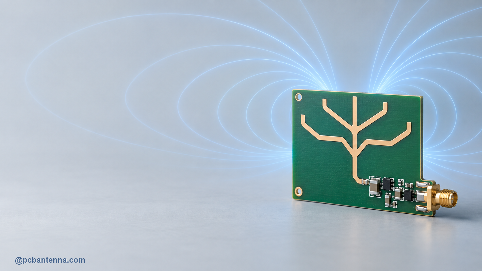
Compact PCB antennas often face a simple physical tension: a smaller radiator usually has less room to support a broad impedance response. When a design needs more bandwidth, the right answer is not automatically a more complicated trace. First identify whether the limitation is geometry, ground plane, matching, enclosure detuning, loss, or an unrealistic band requirement.
Write the required frequency range, reference impedance, and acceptance target in one place. Check the actual radio channels and regional variants rather than assuming a broad band is always needed. A clear requirement prevents unnecessary compromises in antenna size, cost, and efficiency.
Then measure the existing design. Capture S11 or return loss over the whole range, record the enclosure condition, and compare the result with the original reference layout. If the resonance is simply shifted, the best answer may be retuning. If the resonant behavior is inherently too narrow, a different antenna topology or board arrangement may be needed.
Many bandwidth problems begin with layout rather than antenna theory. Restore the manufacturer-recommended keepout, preserve the intended ground plane, keep metal and cables away from the radiator, and use a short controlled-impedance feed. A compact antenna needs its surrounding board space as much as it needs its visible trace.
Review the clearance on all layers. A ground fill added below a chip antenna, a battery cable crossing the antenna, or an enclosure wall placed too close can narrow or shift the useful band. Read how plastic enclosures and batteries detune antennas before changing the copper geometry.
A matching network can move and reshape the input match, but it cannot create radiation efficiency that the physical antenna does not have. Keep the network close to the feed and leave a practical tuning footprint. When the board and enclosure are stable, adjust it based on calibrated measurements rather than by trial and error.
Matching components also have tolerance and loss. A solution that depends on a highly sensitive value can be difficult to reproduce. Prefer a design with reasonable manufacturing margin, especially when the antenna will be produced in large quantities.
Slots, branches, altered ground shapes, and multiple resonant paths can broaden the observed response. They can also introduce new tradeoffs in size, pattern, efficiency, and tuning sensitivity. Use simulation to compare a short list of physically sensible options, then validate on hardware.
A good first experiment is a focused parametric sweep of the radiator length, feed position, or slot geometry. Do not vary every dimension at once. The parametric sweep optimization guide shows how to keep that work interpretable.
Sometimes a compact antenna cannot cover the desired band with the desired efficiency inside the available volume. That is a design constraint, not a failure of tuning. A different chip antenna, an external antenna, a larger board edge region, or a different product placement may provide a more reliable solution.
Compare candidate antennas using their full reference layouts and final-device measurements. A small ceramic component may save board area but require strict clearance. A printed trace may reduce part cost but need more edge length and a carefully controlled ground plane. See ceramic chip antenna versus PCB trace antenna for a practical comparison.
Do not sign off on bandwidth with only an open-board VNA trace. Test the final casing, battery, cable routing, mounting orientation, and intended user interaction. Compare more than one unit when component and board tolerance could matter. A slightly less impressive bench result that remains stable in the product is often the better engineering choice.
Use the antenna calculators for preliminary work, then verify the complete design with measurement. For a review of compact-device constraints, contact PCB Antenna.