Get "10 RF Design Principles Every Engineer Should Know" Free
Learn practical principles for better RF circuits, PCB layouts, simulations, measurements, and troubleshooting.

A practical inverted-F antenna design guide covering PCB layout, ground planes, tuning, matching, measurement, and common mistakes.
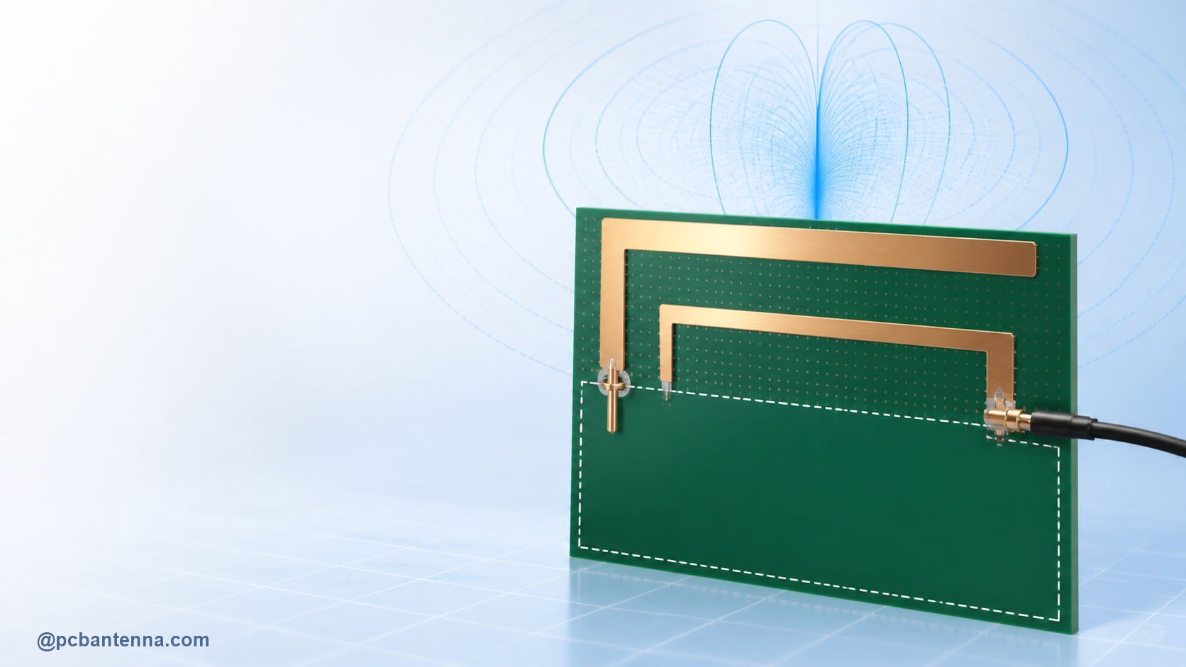
An inverted-F antenna, often shortened to IFA, is one of the most useful antenna shapes for compact wireless products. It can be printed directly on a PCB, tuned for a target band, and integrated without the height of a full external whip. It is also easy to get almost right. A trace that looks sensible on the layout can shift badly once a battery, display, cable, enclosure, or hand enters the picture.
This guide walks through the practical decisions that matter most: what an inverted-F antenna is, how its layout works, what to tune first, and the common mistakes that waste prototype cycles. The goal is a repeatable process, not a magic trace shape.
The classic inverted-F shape has a radiating element, a shorting connection to ground, and a feed point placed between them. The arrangement gives the antenna its characteristic F-like geometry and lets a designer move the feed point to obtain a practical input impedance. In a handset or compact IoT board, the surrounding ground plane is not merely a reference conductor. It is part of the antenna system and can contribute strongly to the final radiation pattern.
You will often see the related term PIFA, or planar inverted-F antenna. A PIFA is an inverted-F implementation with a three-dimensional or elevated planar radiating element. The underlying tuning ideas are similar, but the available height, volume, and ground-plane interaction are different. Do not copy a PIFA drawing onto a flat two-layer PCB and expect the same result.
Before drawing the antenna, write down the operating band, available board area, enclosure material, battery position, cable paths, and likely user orientation. That short list rules out many bad decisions early. A small Bluetooth board, a Wi-Fi product, and a sub-GHz sensor can all use an inverted-F style, but the useful electrical length, ground-plane requirement, bandwidth target, and enclosure sensitivity will be very different.
A quarter wavelength is a useful first scale check, not a finished layout dimension. The effective wavelength changes with geometry, substrate, nearby conductors, and fringing fields. Use the Wavelength Calculator and Antenna Length Calculator to establish a starting scale, then make room for tuning. If the layout leaves no trace-length adjustment or matching footprint, the first prototype becomes much harder to rescue.
Start by measuring the unpopulated or minimally matched antenna in a repeatable setup. Calibrate the VNA as close to the feed as practical, keep the cable position stable, and use the final product enclosure whenever possible. Read our S11 and return loss guide if you need a refresher on what the trace is showing.
If resonance is too low, the antenna is often electrically long or more heavily loaded than intended. If it is too high, it is often electrically short. That is a useful direction, not a substitute for measurement. First adjust the radiating path or the structure responsible for the resonance. Then use the matching network to bring the impedance toward the radio’s target, commonly 50 ohms. Trying to solve a large frequency error only with matching components can reduce efficiency and hide the real layout issue.
After each change, record what moved: resonant frequency, bandwidth, matching depth, and the physical edit. This simple discipline prevents circular tuning. Once the feed match is acceptable, validate with radiated measurements or a realistic over-the-air test. A good S11 curve only says the feed is accepting power; it does not guarantee that the product radiates efficiently or in the right directions.
Full-wave simulation is excellent for comparing layout options before fabrication, especially when you include the board outline, ground layers, key metal, and enclosure features. It becomes less trustworthy when a model omits the things that dominate the device. Keep the simulation goal narrow at first: identify resonance, feed impedance, and likely current distribution. Then compare it with a measured prototype and update the model where needed.
The Microstrip Patch Antenna Design Guide is worth reading for another example of how feed, substrate, and ground influence a planar antenna. For an inverted-F design, the geometry differs, but the engineering habit is the same: design the complete RF structure, not one isolated trace.
An inverted-F antenna is compact because it uses the PCB and ground plane intelligently. That same advantage makes it sensitive to layout decisions. Give it a protected zone, a deliberate feed and short, an accessible matching network, and a tuning process based on the finished product. When the design needs a second set of eyes, contact PCB Antenna for engineering support or explore the full antenna calculator collection for early design checks.